Hi
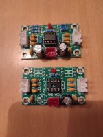
A friend ask me for a cheap buffer for class D chip which recommended a buffer because of low impedance of the power amp ips. i decide to by the cheap XH-A902 dual opamp pcb on aliexpress..i expect that the opamp is fake and not a real one.
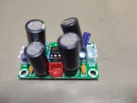
XH-A902
i try to find a schematic but i found nothing and did reverse engineering. it is single supply.
input( R-GND-L) is left side if the power connector is on the buttom. output is R-L mirrored and on a 3 pin connector.
ground from signal in and signal out is decoupled with a 1µF ceramic (yellow in the middle of the 3 caps).
the opmap was checked over the quiecent current and it is not a NE5532. it draws 4mA...a real suck about 10mA.
according to my short search it could be a RC4558. i dont care...i use my NE5532
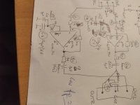
can this schematic work?
yes...(i expect not an inverted amp , there is no voltage divider on the non inverted input...?)
i changed the fb resistor to 2k2 and so i get a gain about 1.
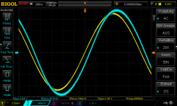
i did a short measurement but the low frequencies down from 400Hz get very fast with low value.? why?
i changed the inputcap with a 10µF and the output cap (after opamp and 1k) with 10µf too. this doesn't t help.
any thoughts?
thank you
chris
A friend ask me for a cheap buffer for class D chip which recommended a buffer because of low impedance of the power amp ips. i decide to by the cheap XH-A902 dual opamp pcb on aliexpress..i expect that the opamp is fake and not a real one.
XH-A902
i try to find a schematic but i found nothing and did reverse engineering. it is single supply.
input( R-GND-L) is left side if the power connector is on the buttom. output is R-L mirrored and on a 3 pin connector.
ground from signal in and signal out is decoupled with a 1µF ceramic (yellow in the middle of the 3 caps).
the opmap was checked over the quiecent current and it is not a NE5532. it draws 4mA...a real suck about 10mA.
according to my short search it could be a RC4558. i dont care...i use my NE5532
can this schematic work?
yes...(i expect not an inverted amp , there is no voltage divider on the non inverted input...?)
i changed the fb resistor to 2k2 and so i get a gain about 1.
i did a short measurement but the low frequencies down from 400Hz get very fast with low value.? why?
i changed the inputcap with a 10µF and the output cap (after opamp and 1k) with 10µf too. this doesn't t help.
any thoughts?
thank you
chris
Attachments

I wonder if that input coupling cap is type II ceramic? If its really 1µF into 2k, then there's a cutoff at 80Hz you really don't want...
The way you've plotted the diagram it looks like the non-inverting input has no DC bias path, so I'd double check that.
The ground coupling cap should be significantly larger than the signal couplers I reckon to limit inter-channel crosstalk.
The way you've plotted the diagram it looks like the non-inverting input has no DC bias path, so I'd double check that.
The ground coupling cap should be significantly larger than the signal couplers I reckon to limit inter-channel crosstalk.
Why so complicated ?
What impedance you need to drive ?
Why not just use OPA1622 as follower ?
Patrick
What impedance you need to drive ?
Why not just use OPA1622 as follower ?
Patrick
thanks Patrick.
but i want to have it cheap -my friend gets the amp for free -if you wants to improve he has to decide his new OPAMP. 😉
chris
but i want to have it cheap -my friend gets the amp for free -if you wants to improve he has to decide his new OPAMP. 😉
chris
Good morning
i wonder what the opamp is directly doing at pin 1 -that was much better but still not acceptable low fq.
that was the trick ! -thanks
The ground coupling cap should be significantly larger than the signal couplers I reckon to limit inter-channel crosstalk.
i solder parallel on each signal input to GND a 220µF lytic cap and the frequency response is not nice!
gain with 2k2 1,2dB, low fg = 7Hz, fg high is clean about 500kHZ with NE5532. 😎
at 1khz i get 2,60Vpp so 70%= fg= is about 1,81Vpp
thanks you guys!
chris
Attachments
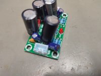
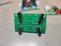
final pics...looks strange because i have just 220µF 35V nothing with less Voltage-they are too big.😆
input caps are panasonic bipolar lytic
input caps are panasonic bipolar lytic
Attachments
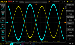
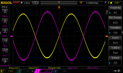
ooops...it was a mistake...the load with 6k was not properly connected...sorry
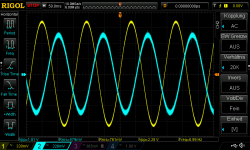
here is the maximum into that buffer without clipping or strange sine wave.
2,5Vrms with 220kHz load (please remember with 2k2 fb resistor i have got about 1,21 gain)
good night
chris
here is the maximum into that buffer without clipping or strange sine wave.
2,5Vrms with 220kHz load (please remember with 2k2 fb resistor i have got about 1,21 gain)
good night
chris
Attachments

possible change of OPAMP on this pcb was not nice---> so new one.
i tested the fake NE5532 and just got on the same conditions as shown above just 80kHz and with just 2,3Vrms input a clean signal. more frequency or more value of the signal give me a more likely triangle signal.
i tested the fake NE5532 and just got on the same conditions as shown above just 80kHz and with just 2,3Vrms input a clean signal. more frequency or more value of the signal give me a more likely triangle signal.
Attachments

hi,
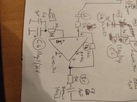
i also tried to identify the schematic of this cheap circuit. it seems just an inverting opamp with some peculiarities and not an phono one.
the ground is made with two sets of series caps and a potential divider. and having decoupling caps both on input and outputs but also in series with the signal grounds probably to prevent accidental schortcircuits due to the way the voltage supply may be available in the various usages. but is not really a PHONO/RIAA amplifier
That circuit is a classic non inverting gain stage. Gain is (20k/2k)+1 which is 11
The caps on the virtual ground are to maintain a low supply impedance and all the signal caps are needed because the circuit is biased to one half the supply voltage by the virtual ground and so can not be DC coupled.
The caps on the virtual ground are to maintain a low supply impedance and all the signal caps are needed because the circuit is biased to one half the supply voltage by the virtual ground and so can not be DC coupled.
no, is inverting. signal goes to pin 2 not 3. and is not biassed. if it was DC biased on the input, then one should have seen the mid point added to the input and also have a capacitor in series on the grounding resistor to give zero gain in DC
It can be configured either way. Connect the + input to the virtual ground and apply the signal to the 2k and you get an inverting amp of x10 gain but with a low input impedance.
The non inverting configuration does need a bias resistor from the + input to the virtual ground.
The non inverting configuration does need a bias resistor from the + input to the virtual ground.
- Home
- Source & Line
- Analog Line Level
- Chinese opamp PCB XH-A902