 This thread has been split from here - https://www.diyaudio.com/community/threads/beast-with-1000-jfets-redux.364186/
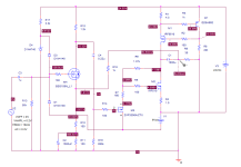
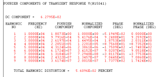
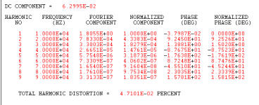
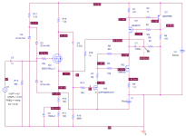
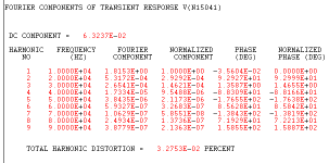
I played with the idea in sim, and ended up with a design using all mosfets, not a jfet in sight. It uses a "fake SIT " pair at the output, using an IRF510, , a ZVP3306A, and a couple of resistors to mimic the triode-ish behavior of a SIT. I drive the SIT with a ring-of two current source using a small signal PNP and an IRF9510. There's my favorite depletion mode mosfet at the input, the Infineon BSS159, and I close the loop from the output to the BSS159 source. Distortion sims at about 0.05%, mostly 2nd harmonic, and gain is about 10X., about the right gain for a headphone amp. I may grab a pair of Audio Technica studio headphones, as they look to sit more comfortably on the ear than the Grados I currently own.
Last edited by a moderator:

Changing the resistor at the gate of the BSS159 from 100 ohms to 10k seems to get the job done compensation-wise. This time around, Mr. Miller is working in my favor for once…

Last edited by a moderator:
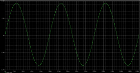
Having said that, through, I'll be giving the finished product a workout with the gain-phase analyzer at my work place, as the time domain response doesn't necessarily tell the whole story. I want to make sure that the output response crosses through zero dB at some point and stays down.
Restricting the input bandwidth doesn't change the stability (either good or bad) of the amplifier circuit.
A small capacitor, around a few nF, across R16 should clean it up, instead of hiding the problem by restricting the input BW.
A small capacitor, around a few nF, across R16 should clean it up, instead of hiding the problem by restricting the input BW.
The gain phase analyzer will tell the tale. Despite your quibbles, I'm building this thing.
The BSS159 is also serving as the summing node for the global feedback,, so restricting its bandwidth will have an affect on the global feedback. Again, I'll be checking the finished product with a bona-fide gain-phase analyzer, so I will find out one way or the other.
The BSS159 is also serving as the summing node for the global feedback,, so restricting its bandwidth will have an affect on the global feedback. Again, I'll be checking the finished product with a bona-fide gain-phase analyzer, so I will find out one way or the other.
Last edited:
The picture I show in post 410 is from the output of the amp, so changing the bandwidth at the input summing node is having an overall effect on the output response.
'Beast' is based on how many precioust toshiba jfets were wasted for few watts 🙂
NP has pallets full of those.
I am confused by R10 and R11 in post #408. They appear to connect between an ideal voltage source (-6.0000 volts) and ground, but the midpoint is a positive voltage, above ground? Howzatt ?
_

_
Last edited by a moderator:
Having learned from sad experience, I wanted to tie the drain of the P-Channel mosfet to a negative source for some reliable turn-off drive. I will generate the negative supply using some sort of voltage multiplier scheme and a zener diode, tapped off the main XFMR winding supplying the +24V.
The output voltage at the center point is governed by the ratio of R6 and R7. The combination of the N-Channel mosfet, the P-channel small-signal mosfet and R6 and R7 act like a rough approximation of a triode/SIT.
The output voltage at the center point is governed by the ratio of R6 and R7. The combination of the N-Channel mosfet, the P-channel small-signal mosfet and R6 and R7 act like a rough approximation of a triode/SIT.
Last edited:
R10 and R11 are used to set the bias current in depletion mode mosfet M4. I split the resistor and bypassed part of it for more open loop gain. D1 is hooked to the -6V voltage source for gate protection. I will generate the -6V supply using some sort of voltage multiplier scheme off the main winding that generates the 24V, with a smallish input cap to strangle the current capability of the multiplier circuit.
Last edited:
I don't quite see how it can be possible to measure a positive voltage at the junction of R10 and R11? One side is ground, the other side is -6.000 volts, and the middle is +0.96 volts??? Really?
_
_
I do not believe there is connection of the -6V to the mosfet source and source resistor R10.

Last edited by a moderator:
- Home
- Amplifiers
- Pass Labs
- Wrenchone's MOSFET Headphone Design