Dear Members,
I have an old, simple PMA320A in wich I made some repairs because of age and the all-time failing phono stage. I must note that the +15 V supply have failed and it was around +30 V of +VCC supply on every opamp and the input selector for maybe years (the slight noise on every input selection was there with this amp since years and it is cured with the right supply voltage) and every parts have survived it, with no apparent problem with operation!
So back to the topic, this is a revised amplifier (denotes "A"), with opted out over temperature protection and a slightly reworked PCB. The topic is bias circuit. Let's see:
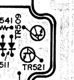
This is a bit uncommon biasing, TR521 serves as a diode and in series with TR509, forms a Vbe multiplier with an added extra thermal compensation of the Vbe multiplier. The two transistors are mounted near the heatsinks and covered with some compound to help heat detection (not the most beautiful solution), as can be seen on the left side of the circuit:
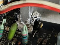
Until this point everything looks fine. But let's see left side on the PCB:
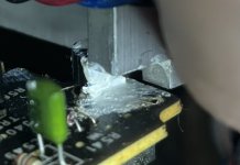
As You can see, somebody is missing. Only one transistor is mounted (the Vbe multiplier), the other holes are unpopulated. See the PCB side, it is made this way in the factory, and one can quickly realise that the drawing is faulty, there is no connection to the (wrongly aligned) common B-C legs:
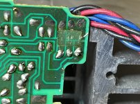
However the B leg of TR509 goes down the way on the PCB, where...
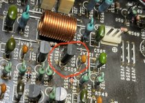
..it arrives under TR515 driver and a diode D509 (not visible on the shcematics anywhere else, so maybe the solution existed before..) is placed here (it is already removed by me). Let's see it on drawing, what Denon did:
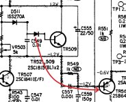
(The resistor next to D511 was also altered to a smaller value not visible on the picture).
So it looks like somebody made an error, also tried another solution for heat compensation, and the two things have mixed up not only in PCB, but in schematics too. And indeed, the thermal point and biasing was so different between the two sides that I started to suspect some nasty errors around, but finally I found this difference. It is very interesting for me, that what and how happened. The layout can be easily converted back to the original solution, the extra transistor can be added (I have used an european made one because the layout -EBC- fits the right way with the badly aligned PCB for layout -BCE-) and the diode can be left unpopulated and linked.
Maybe some trial test PCBs, maybe went out for production? I have seen few images from other 320A amps and those all have this weird solution.
Any comments, or ideas?
I have an old, simple PMA320A in wich I made some repairs because of age and the all-time failing phono stage. I must note that the +15 V supply have failed and it was around +30 V of +VCC supply on every opamp and the input selector for maybe years (the slight noise on every input selection was there with this amp since years and it is cured with the right supply voltage) and every parts have survived it, with no apparent problem with operation!
So back to the topic, this is a revised amplifier (denotes "A"), with opted out over temperature protection and a slightly reworked PCB. The topic is bias circuit. Let's see:

This is a bit uncommon biasing, TR521 serves as a diode and in series with TR509, forms a Vbe multiplier with an added extra thermal compensation of the Vbe multiplier. The two transistors are mounted near the heatsinks and covered with some compound to help heat detection (not the most beautiful solution), as can be seen on the left side of the circuit:


Until this point everything looks fine. But let's see left side on the PCB:

As You can see, somebody is missing. Only one transistor is mounted (the Vbe multiplier), the other holes are unpopulated. See the PCB side, it is made this way in the factory, and one can quickly realise that the drawing is faulty, there is no connection to the (wrongly aligned) common B-C legs:

However the B leg of TR509 goes down the way on the PCB, where...

..it arrives under TR515 driver and a diode D509 (not visible on the shcematics anywhere else, so maybe the solution existed before..) is placed here (it is already removed by me). Let's see it on drawing, what Denon did:

(The resistor next to D511 was also altered to a smaller value not visible on the picture).
So it looks like somebody made an error, also tried another solution for heat compensation, and the two things have mixed up not only in PCB, but in schematics too. And indeed, the thermal point and biasing was so different between the two sides that I started to suspect some nasty errors around, but finally I found this difference. It is very interesting for me, that what and how happened. The layout can be easily converted back to the original solution, the extra transistor can be added (I have used an european made one because the layout -EBC- fits the right way with the badly aligned PCB for layout -BCE-) and the diode can be left unpopulated and linked.
Maybe some trial test PCBs, maybe went out for production? I have seen few images from other 320A amps and those all have this weird solution.
Any comments, or ideas?