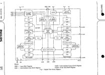
Alright, which one of you brave lads has done the unthinkable and hooked pin 13, TEST, on a SAA7220 to VCC? Nowhere in the datasheet is there any mention of the function of this pin, other than it being pulled low internally? What happens when you hook it to VCC? Did anyone try? Or is this, a good 35 years to date, still unchartered territory? Should I venture there, and risk being pulled into a quantum time vortex and be transported back to Philips' Natlab in the mid 1980's?


I haven't, but it sounds like a scan test enable pin, assuming that scan tests were already used in 1985. If it is, it turns the chip into one or more big shift registers with combinatorial logic in between. You clock your test patterns into the shift register or registers using some pin that has a different function in normal use, parallel load the output of the combinatorial logic into the register and clock it out again.
Nowadays we usually hide those pins better, or use some secret I2C command for it or so. For example, if they had simply called it GNDsomethingorother, customers would simply ground it without even knowing it is really a scan test enable.
Nowadays we usually hide those pins better, or use some secret I2C command for it or so. For example, if they had simply called it GNDsomethingorother, customers would simply ground it without even knowing it is really a scan test enable.