
Some questions:
With only this C1 issue, the amp can be operational (after thourough simu's and mods though).
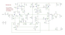
- why a 10:1 divider (R10 R9), now V1 needs to be 10x higher
- why C1 in the (not) ground connection of V1, the offset reference runs through R10 - not the most reliable solution
- why the 470p (C2) over R10
- why this amount of emitter degeneration (R1 R2), there is a second differential to lift the open loop gain also
- the bias opens up to 2 x Vbe of Q? (BD139), but is this enough for the Sziklai's Q? & Q? (2SC4793 2SA1837)
- there will be some offset, caused by the base current of Q? (S9015 right/feedback side); what's the topology choise here
- have you simulated closed & open loop gain & phase response; are there plots available
- most zobel network involves a coil//resistor (present) and a cap+resistor (not) network; why so
- there are four grounds: GND1, GND2, GND3, GND4; these are not four different grounds but one and the same (I hope)
- the drawing is a bit unusual, but readable; only a small size drawing area available
With only this C1 issue, the amp can be operational (after thourough simu's and mods though).
D
Deleted member 550749
D
Deleted member 550749
Removed or changed trsistor names Q1,2 etc , if anyone wants to simulate plz do that, looks like not complex hope experts can complete this to final , 👍

- why a 10:1 divider (R10 R9), now V1 needs to be 10x higher
- why C1 in the (not) ground connection of V1, the offset reference runs through R10 - not the most reliable solution
- why the 470p (C2) over R10
Be carefull see where the groud is ... circuit is not drawn the usual way with ground at the bottom on an horizontal line ...
D
Deleted member 550749
It's just drawing error not simulated ( ground ), actually my big brother has laptop he is always busy in laptop, not able to simulate but anyone can improve it and circuit wil b his 👍 do whatever u want with it just complete it as a project 👍
Hello! in the circuit, the main error is the aperiodicity of the signal from the second differential stage; Even a Wilson current source in the driver stage will not help, because it will conflict with the input stage current mirror. It is also advisable to introduce a signal level limitation into such a circuit, since when the signal is removed in this way, its level increases by the square root of 2.Removed or changed trsistor names Q1,2 etc , if anyone wants to simulate plz do that, looks like not complex hope experts can complete this to final
There are no mistakes there; those who know how to read diagrams will read them upside down.It's just drawing error not simulated ( ground ),
Please....if anyone wants to simulate plz do that, looks like not complex hope experts can complete this to final
Attachments
Thank you very much!Be carefull see where the groud is ... circuit is not drawn the usual way with ground at the bottom on an horizontal line ...
When I realised it, I said something different...
D
Deleted member 550749
Further considerations:
Q3-Q4 current mirror is better omitted, this won't work well together with the differential Q12-Q13. The base of Q12 is more or less fixed, so the current mirror Q7-Q8-Q9 does not contribute to the dc-stability of the amp, which is prime condition over ac-amplification. This dc-stability is now a task of the first stage, which has other duties as well (error regulation, noise, ac-amplification, maybe hf-suppression also but not present).
R9-R10 is a 2:1 divider, a bit sad; with C1 = 10μ, R9 can be 1.0kΩ (Fo~16Hz). Typo?
Try to get the time constants of the input filters (C1-R9-C2-R10) and the feedback network (R11-C4-R12) close to each other, the zero's of the input at least an octave lower than the feedback. A small cap over R12 supresses unwanted hf-instability (aka oscillation). A RC network between the collectors of Q12-Q13 prevents open loop oscillation also (not present).
The bias and choosen output stage (a regular Sziklai, not the inverted Hiraga Sziklai stage!) is a bit awkward: ample regulation/control with very steep transfer. This can have a tendency to run away even if Q11 (bias BJT) is on the heat sink. Daring topology, better for low idle class aB (minuscule-capital!).
A bleeder resistor at the input (C1) prevents plops/bumps/thumps, part of the input network. And a complete Zobel network at the output.
In general, current mirrors are (supply) noise injectors into the signal path, lowering the PSRR considerable. Also a topology choise.
What protection circuits (thermal, SOA, &C) do you have in mind?
Hennady did post (#10) a fine drawing in the classic view with several improvements and some alterations. I have to think about this Q2-Q9 configuration though.
If I have some spare time this weekend, I'll run some simu's (closed/open loop bode plots, startup/shutdown supply) in AimSpice.
And always: have the Sziklai compound thermally separated, no matter what!!!
The D1-D2 path creates a possible DC positive feedback: if the Q1c-R12-R5-Q12b node voltage goes up by a shock (odd reason, thermal issue, whatever), more than the opposite Q4c-R10-Q8b node, the loop is suddenly noninverted causing instability.Please....
This is a clipping protection circuit, the case you are writing is already an emergency mode and the amplifier will not work even if these diodes are removed. You can simulate the circuit with and without these diodes to see if their presence makes sense.The D1-D2 path creates a possible DC positive feedback: if the Q1c-R12-R5-Q12b node voltage goes up by a shock (odd reason,
- Home
- Amplifiers
- Solid State
- Schematic gonna work or not??