Hi,
I am looking for someone that corrects or redesign a simple pcb from an schematic.
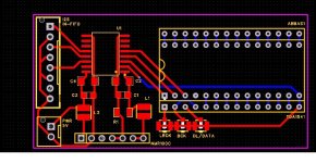
Basically, the board is a kind of breakout board for a TDA1541 dac. This board is installed in the TDA1541 socket and:
1. Routes the TDA I2S input signal to a XH connector. I have placed an isolator to avoid any unwanted ground loop. This isolator is powered with a dedicated psu (independent secondary) and a dc-dc isolator to power both sides.
2. Provides three UFL connectors to connect an I2S signal into the TDA1541 which is installed in the board.
Using this board I can install a FIFO in any TDA1541 DAC without modifying or removing any component. I have build a prototype and it works as expected so I would like to build it seriously but do not the skills to do so.
I have an EASYEDA project I can share.
best regards,
jm
I am looking for someone that corrects or redesign a simple pcb from an schematic.
Basically, the board is a kind of breakout board for a TDA1541 dac. This board is installed in the TDA1541 socket and:
1. Routes the TDA I2S input signal to a XH connector. I have placed an isolator to avoid any unwanted ground loop. This isolator is powered with a dedicated psu (independent secondary) and a dc-dc isolator to power both sides.
2. Provides three UFL connectors to connect an I2S signal into the TDA1541 which is installed in the board.
Using this board I can install a FIFO in any TDA1541 DAC without modifying or removing any component. I have build a prototype and it works as expected so I would like to build it seriously but do not the skills to do so.
I have an EASYEDA project I can share.
best regards,
jm
Attachments
Last edited:
I think there will be no dearth of suggestions for you here.
The long blue trace going to the far end of the large connector can be eliminated,
along with the via, and rerouted as a red trace going directly down to LRCK common.
Then if you move all the remaining blue traces to the red layer,
the blue layer can be a solid ground plane.
The long blue trace going to the far end of the large connector can be eliminated,
along with the via, and rerouted as a red trace going directly down to LRCK common.
Then if you move all the remaining blue traces to the red layer,
the blue layer can be a solid ground plane.
Last edited: