Hi all,
I keep running into people mentioning Blameless amplifier all the time.
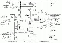
Searching on the internet I could only find schematics from Douglas Self articles.
Is this it? and is there a simple LTSpice simulation that tests all of the parameters?
It was not hard to put one together myself, but I only know so much in LTspice so maybe there can be more suggestions on what to measure?
Maybe this can be a good exercise to learn more about LTspice...
Thanks
I keep running into people mentioning Blameless amplifier all the time.
Searching on the internet I could only find schematics from Douglas Self articles.
Is this it? and is there a simple LTSpice simulation that tests all of the parameters?
It was not hard to put one together myself, but I only know so much in LTspice so maybe there can be more suggestions on what to measure?
Maybe this can be a good exercise to learn more about LTspice...
Thanks
Attachments
Last edited:
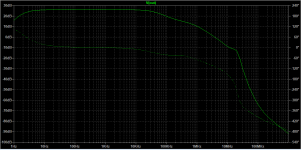


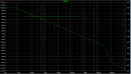
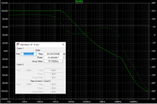
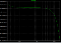
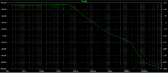
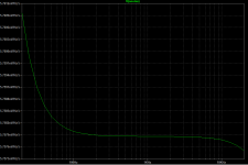
Here I am attaching what I think is open loop gain graph, but people have corrected me before explaining that this is something else....
I am inserting 1 giga henry coil into the feedback path to block the AC and 1 farad cap to bock the DC. Also AC generator in series with the cap.
So the feedback is broken in the AC domain between the output and inverting input.
And DC is blocked from the inverting input to the ground.
AC is then fed into the inverting input.
Attachments
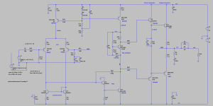
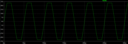
And improved updated version.
Improvements:
THD1 to 0.000037%
THD20 to 0.005%
With 36V power supply output power should be around 100-110W into 4 ohm.
Improvements:
- better and separated constant current sources - added 1k resistor for smooth HF response
- LTP degeneration resistors increased to 200R for nice square wave response working in conjunction with Miller cap of 47p value
- Better precision current mirror allowing for less DC offset voltage at output
- Clipping behavior improved by adding current limiting transistor and base/collector resistors
- Two pole compensation
- Phase lead cap and resistor across the feedback resistor for nice square wave response
- Power rail decoupling
- Rail protection diodes
THD1 to 0.000037%
THD20 to 0.005%
With 36V power supply output power should be around 100-110W into 4 ohm.
Attachments
Last edited:
That's my favourite way of performing loop gain analysis as well. Note, though, that with an AC magnitude of 1 (instead of -1) you get the phase margin indicated on the phase graph, not the phase of the loop gain itself. There's no harm in that. In fact, I often find it more convenient to be able to read the PM directly, but some may grumble.I am inserting 1 giga henry coil into the feedback path to block the AC and 1 farad cap to bock the DC. Also AC generator in series with the cap.
So the feedback is broken in the AC domain between the output and inverting input.
Some may also argue that breaking the loop eliminates the effect of the input stage on the output. That's true, but we're comparing a relatively high-impedance node versus the output of the amp that's decidedly low-impedance. I think this is a good spot for breaking the loop.
Tom
If the amplifier's input-to-output gain is "G" volts per volt,
then the tail node of the input differential pair swings, at most, plus-or-minus (RailVoltage / G) volts above and below ground.
So for example if the rail voltage is 37 volts and the gain is G = 11 volts per volt: then the tail node swings plus-or-minus 3.37 volts, above and below ground.
Thus the voltage across the current source which applies current to the tail node of the input differential pair, is (37 - 3.37) = 33.63 volts or greater.
Therefore, if you wish, you can EAT UP A WHOLE LOT OF VOLTS OF HEADROOM across the input stage current source. Put 200 * (kT/q) volts across the emitter degeneration resistor. Put 5V across the outermost (rail-facing) transistor in the cascode. Put 20+ volts across the cascode transistor. You've got voltage headroom out the wazoo. Squander it. Invest it. Use it to your advantage.
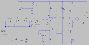
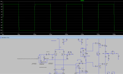
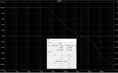
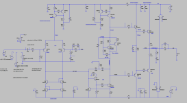
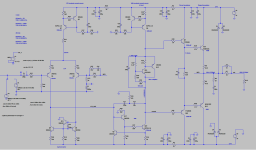
Here is the complete schematics for the LG measurements that I was using.
I am still trying to figure out how to measure exact phase margin.
Tried with both AC at 1 and -1.
I am still trying to figure out how to measure exact phase margin.
Tried with both AC at 1 and -1.
Attachments


Last edited:
What do you suggest? Ripple eaters aka cap multipliers? Better CCSs?Use it to your advantage.
Perhaps the state of the art:
https://sites.google.com/site/frankwiedmann/loopgain
Note that this is illustrated in the example files: %USERPROFILE%\Documents\LTspiceXVII\examples\Educational\LoopGain2.asc
But I get essentially the same results as long as I put the simple Va/Vb probe in the usual spot, and you can use the .measure directive to find the gain and phase margin.
.meas AC PhaseMargin FIND V(A)/V(B) WHEN mag(-V(A)/V(B))=1
results in the error log.
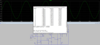
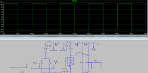
Noise measurement setup attached.
Output had to be normalized by the value of the gain to compare noise contribution (using E1).
15.3 nV/Hz^1/2
Just for the comparison, LM4562 has noise of 4.7 nV/Hz^1/2
Output had to be normalized by the value of the gain to compare noise contribution (using E1).
15.3 nV/Hz^1/2
Just for the comparison, LM4562 has noise of 4.7 nV/Hz^1/2
Attachments
Last edited:
Replacing current mirror with three transistor version halves the noise. Reducing input resistor from 1k to 100R bring the noise down to 6.5 nV/Hz^1/2.
Attachments
Last edited:
Tom,That's my favourite way of performing loop gain analysis as well.
LTspice has an example file showing how to use the Tian probe (LoopGain2.asc). I've used this with success, although I'm also familiar with the large L and large C approach. Is there a reason you prefer the latter over the Tian method?
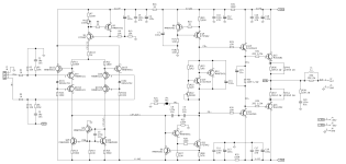
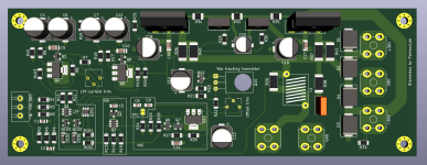
I am moving forward with this amplifier and capturing schematics in KiCAD now, but I am having a few concerns.
First of all, I want this to be able to accept balanced input signal from my topping DAC.
Second, I am hoping to get rid of input DC blocking capacitors and so maybe utilize a servo.
But for now, here is what I came up with for the input -
Using two opamps as unity buffers and having Long Tailed Pair of transistors sum up the positive and the negative swings of the signal.
What I don't know is to how to measure CMRR of the setup.
I tried having 1V of offset on the inputs and it moved output 20V down.
I also tried having DC blocking cap of 2.2uF film type and it seems to solve the offset issue.
Attachments
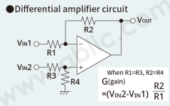
There are multiple benefits of having balanced connections to the amplifier.
Most significant in my opinion is the separation between the ground wire and the signal.
No electrical ground is 100% clean so it would make sense to electrically separate signal path from going through the ground.
But at some point differential signal has to be converted to be accepted by the conventional amplifier.
With that in mind, I have decided to use LTP design that allows for balanced inputs.
Meaning amplifier is connected as a difference amp.
Meaning that LTP is now performing multiple tasks.
Including combining two differential signals.
And the usual comparing between input signal and NFB signal.
Adding cascoded and bootstrapped LTP does not require that many expensive parts.
But improves on THD performance which was verified in the simulator.
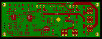
PCB layout was finished and now being verified and hopefully will order those PCBs soon.
Super excited about this project!
Most significant in my opinion is the separation between the ground wire and the signal.
No electrical ground is 100% clean so it would make sense to electrically separate signal path from going through the ground.
But at some point differential signal has to be converted to be accepted by the conventional amplifier.
With that in mind, I have decided to use LTP design that allows for balanced inputs.
Meaning amplifier is connected as a difference amp.
Meaning that LTP is now performing multiple tasks.
Including combining two differential signals.
And the usual comparing between input signal and NFB signal.
Adding cascoded and bootstrapped LTP does not require that many expensive parts.
But improves on THD performance which was verified in the simulator.
PCB layout was finished and now being verified and hopefully will order those PCBs soon.
Super excited about this project!
Attachments
That design assumes its driven by low impedance, it might even be unstable without an input, the feedback current is forced into the inputs exposing any non-linear impedances in the driving equipment, as well as being well below the nominal line impedance, which could mean DC-blocking caps might reduce the bass response if they have been chosen with 47k load in mind.
I think its better to go with something like an instrumentation amp circuit that provides high impedance load and does differential->single ended conversion with reasonably low noise. You can even add some gain.
I think its better to go with something like an instrumentation amp circuit that provides high impedance load and does differential->single ended conversion with reasonably low noise. You can even add some gain.
You are correct.
This is not a complete solution.
I am planning on adding buffering board that will have XLR connectors and LM4562 unity gain followers.
And DC blocking caps at the XLR input. Something like 3.3uF with 47K resistor.
Along with 15V regulators.
I am still thinking about the servo.
Although unity buffers should not have that much offset voltage and also, there is offset adjust on the board.
Going back to simpler design gives pretty much the same distortion.
So why complicate?
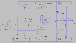
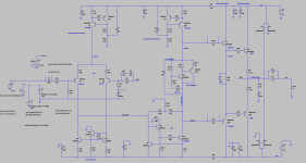
Attached is updated simulation with exact transistors that I plan on using for the build.
All transistor models were loaded into the simulation.
Revised compensation a little.
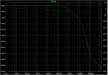
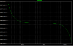
15W 1kHz THD: 0.000141%
15W 20kHz THD: 0.00085%
Noise is 5.76 nV/Hz^1/2
So why complicate?
Attached is updated simulation with exact transistors that I plan on using for the build.
All transistor models were loaded into the simulation.
Revised compensation a little.
15W 1kHz THD: 0.000141%
15W 20kHz THD: 0.00085%
Noise is 5.76 nV/Hz^1/2
Attachments
I think the output part should be three-level. for low impedance speaker systems will be better in terms of distortion...
will be pretty similar to what I simulated and named Cordell -1
https://www.diyaudio.com/community/...age-by-bob-cordell.390124/page-2#post-7127035
message # 11
will be pretty similar to what I simulated and named Cordell -1
https://www.diyaudio.com/community/...age-by-bob-cordell.390124/page-2#post-7127035
message # 11
Last edited:
- Home
- Amplifiers
- Solid State
- Is there a simple one-to-one simulation for Blameless amplifier in LTspice?