Hello everyone! I was wondering if you could help me out.
A while ago I took on the challenge to build myself a quad NAD 3020 power amp with an ESP 4 way crossover, and a NAD 1020 pre amp. Without tone section, but with the 1020/3120 high level pre-out. Which would make this a NAD 1120 if you like. I know I do 😉
Clone power amp and PSU PCB's I purchased from Scafas.
I also bought a Chinese clone of the pre amp, but I thought it would me more fun to make this myself.
And so it began...
This is the first time I am making a PCB. A challenging task I must say!
After a lot of time fiddling around with Circuitmaker I came up with something I think I'm happy with. One channel only for now.
I really don't know if it's any good. Could you shed your light on this design for me please?
Questions I have:
PCB version with and without Gnd plane added, for visibility tracks on back layer
Thanks a bunch!
A while ago I took on the challenge to build myself a quad NAD 3020 power amp with an ESP 4 way crossover, and a NAD 1020 pre amp. Without tone section, but with the 1020/3120 high level pre-out. Which would make this a NAD 1120 if you like. I know I do 😉
Clone power amp and PSU PCB's I purchased from Scafas.
I also bought a Chinese clone of the pre amp, but I thought it would me more fun to make this myself.
And so it began...
This is the first time I am making a PCB. A challenging task I must say!
After a lot of time fiddling around with Circuitmaker I came up with something I think I'm happy with. One channel only for now.
I really don't know if it's any good. Could you shed your light on this design for me please?
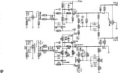
- I copied the circuits from the service manuals and more or less followed the original PCB layout
- I took the original NAD3020 pre amp section (with the benign crosstalk error). Rail voltages +29,9V and - 25,6V
- ripped out the tone section
- added the 1020 hi level pre out. That one runs on +-20V.
- and hooked them up together, using the rail voltage of the 3020.
Questions I have:
- is it possible to increase rail voltage on the high level pre out from 20V to 30V without changing resistor values? (R5xx)
- Could you check on the value of resistors R541 and R539? I think I might have muddled this up.
PCB version with and without Gnd plane added, for visibility tracks on back layer
Thanks a bunch!
Attachments
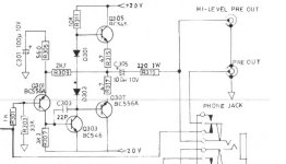
Shouldn't R301 feed directly from C517, otherwise load currents from the Pre Out connector will impose voltages across R541...?
Those tiny thin traces will break very easily if that's a one-sided PCB, or if its a 2-sided, some of the tracks that split ground-plane can be routed on the other side... Why are the transistors at strange angles?
Those tiny thin traces will break very easily if that's a one-sided PCB, or if its a 2-sided, some of the tracks that split ground-plane can be routed on the other side... Why are the transistors at strange angles?
hey Mark. thx! you're probably right. R541 seems to be a resistor in the sw-7 (mute) circuit. (which I omitted)
It's a 2 sided PCB. Will see if I can put the tracks that split GND plane on the back side. Autoroute didn't.
I angled some of the transistors to find shortest path, before routing.
It's a 2 sided PCB. Will see if I can put the tracks that split GND plane on the back side. Autoroute didn't.
I angled some of the transistors to find shortest path, before routing.
Last edited:
Hello NPNL!
Nice that you took the time to recreate the NAD 1020. I've looked into the design a bit and have some suggestions.
I did notice that you incorporated the Loudness switch. In the original the loudness switch is connected to a center tab on the volume control potmeter. Bit hard to read on the original schematics. These potmeters are almost impossible to find (and even more so if you want a quality ALPS knob as they don´t exist). So I omitted loudness in my own recreation of the 3020 and just removed the entire section and go without loudness.
You already mentioned that the ground plane could be better. I think it could indeed be filled below all the components, like Mark mentioned. Maybe rearrange some of the traces a bit and you're good to go. And you can always interconnect top and bottom using via's if you find that some of the gronud planes are not connected in places. It also looks like there is a lot of clearance between some netclasses, that might be the reason the ground plane is so small?
Furthermore, if you are going to hand solder the pads it might be a good idea to increase the size of the pads just a little bit as well. And while you're at it the thermal relief on those pads plus the traces are also a bit small, at least for my liking when hand soldering. I usually increase all the default trace widths just to make it a bit more beefier for home etching and soldering.
Really it's a shame that Europe in general doesn't have a cheap option for prototyping PCB's. For me personally I have not really been working with ground planes and double layered PCB's since my designs are usually one layer boards anyways. With single layered board its also much harder to route the traces so you'll become very good at it 🙂. It's oldschool I know but that allows me to make prototypes on the fly using photosensitive copper PCB's with transparent sheets and whatnot. It's a tedious and messy process but it kinda works really well if you get the hang of it. And the results can be just as good!
But love to see how this ends up and how the boards look (and would love to know if the PCB process went smooth)!
Greetings
Johan
Hey Johan! Thanks for your careful examination and suggestions!
Didn't know about the center tab for loudness! As it's probably always on I might as well omit the switch.
R1 batch is underway from Hongkong. I will see if the solder pads are big enough for me. Will follow up on your suggestion for GND plane. Will see if I can tighten up on those netclasses for R2.
I'll PM you a photo of the PCB. Ordering process with JLCPCB is really smooth once you get the hang of it. They have a good tutorial for configuring the Gerber files. ... which you have to follow up on... and don't forget to outline the board 😉 The accountmanagers will gladly point that out to you.
I think I prefer that to spilling etching fluid all over my desk.
I'm working on the phono section now. MC/MM. Will see if I need your hack as well!
First, let's order some components now! 🙂
Are you still happy with your 3120?
Last edited:
- Home
- Source & Line
- Analog Line Level
- RFC PCB NAD 3020 inspired '1120' pre amp + hi level pre out