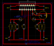
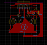
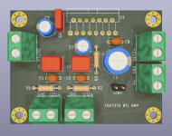
Hi, I was making myself a PCB for TDA7375 ( original from old Blaupunkt car radio ), anyway.
I was wondering if my GND is good or it is a ground-loop . Please take a look.
Also what resistor value to use for bridging the signal and power grounds?.
I was wondering if my GND is good or it is a ground-loop . Please take a look.
Also what resistor value to use for bridging the signal and power grounds?.
Attachments
Last edited:
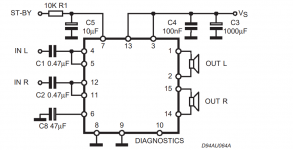
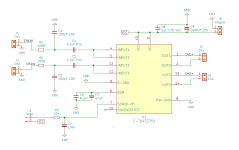
This is the schematic from Datasheet, compared to the schematic from the CD player.
it has 4.7u instead of 0.47 input caps, additional 4.7k res with 100p to gnd (high pass I assume or. )
4.7k input resistors , and 100p caps between each output ? I dont know for what, stability from long wires? .
I dunno if its " better" then the Datasheet schematic, or which one should I make.
it has 4.7u instead of 0.47 input caps, additional 4.7k res with 100p to gnd (high pass I assume or. )
4.7k input resistors , and 100p caps between each output ? I dont know for what, stability from long wires? .
I dunno if its " better" then the Datasheet schematic, or which one should I make.
Attachments

Yeah... definitely.
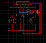
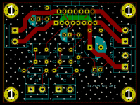
I have neatened up the original PCB layout (was hardly visible). I have also provided the place to insert the ground lift resistor, but I believe it will not be required in this instance. If it is not required, just link the two "X" points. Also, I marked the preferred place to connect the power supply negative (or zero).
NOTE: the C8 in the circuit diagram is in fact C6 on the PCB layout. The link between C6 positive and pin 6 was not really visible at all on the PCB layout - fixed that as well. In addition, I fixed the PCB layout around SW1.
Otherwise, the PCB layout as provided by the manufacturer is textbook perfect. I may have the tiniest of remarks... but it is really good... for audio amplifier applications.
I also placed the IC pin numbers there.... just to make life easier.
@Extreme_Boky @tomchr
Thank you ! But Please can you explain what is wrong with my design ? is it not good to have the GND around the board like in post 1?
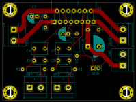
Would this be better ?.
- is this the ground plane you talked about?
Thank you Extreme_Borky for your time to edit that pcb from the datasheet.
Thank you ! But Please can you explain what is wrong with my design ? is it not good to have the GND around the board like in post 1?
Would this be better ?.
- is this the ground plane you talked about?
Thank you Extreme_Borky for your time to edit that pcb from the datasheet.
Attachments
I'm not saying that you're WRONG because there's room for more nuance than a RIGHT-WRONG dichotomy.
Lower impedance is better. Lower impedance -> wider, shorter traces. The widest trace you can get is a plane, i.e. a completely flooded copper layer. The challenge then is that you also want to keep the sensitive ground nodes away from the high current paths. One approach to doing that is what you show in Post #7, except you might want to keep the feedback current separate. Also, there's plenty of room for more copper on the PGND. You're paying for the copper anyway so you might as well use it.
You'll probably find this post useful: https://www.diyaudio.com/community/threads/extra-lm3866-components.394272/post-7234653
This may be helpful as well: Taming the LM3886 - Grounding. I do understand that you're not working with an LM3886 but the physics that govern the TDA7375 are the same as those that govern the LM3886.
Also, don't forget to add mounting holes.
Tom
I see reference layout got s-gnd directly connect to pin 9, p-gnd to pin 8. I think not need connect two gnd by resistor, or better just connect pin 8 & 9 together.
The layout in post1 looks fine, just need to increase the size of the gnd lines.
The layout in post1 looks fine, just need to increase the size of the gnd lines.
Do not just connect pins 8 and 9 together... Do it exactly as per post#5. The current amount flowing into pin 8 is the sum of all speaker currents. It could be as much as a few amps.
... do a Google search for "proper grounding technics in audio amplifiers".
Edit: here are a few documents to get you started...
... do a Google search for "proper grounding technics in audio amplifiers".
Edit: here are a few documents to get you started...
Attachments
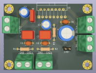
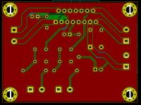
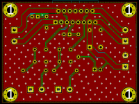
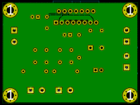
I just wanted to pitch in my solution here.
I am attaching screenshots of how I would do it. Two layers board, 0.3mm tolerances and min traces, bottom is GND, top is signal + power. GND is then poured on top and connected with bottom GND with stitching vias - to improve on EMI and keep all GND area close to 0V.
Really cool youtube channel that I found was very helpful is called Phil's Lab - you can find bunch PCB tutorials there.
Attached is also a gerber file that can be uploaded for the PCB to be produced at for example JLCPCB or any other manufacturing. Screenshots kind of show my process of how I would design step by step.
Board size is 45mm x 60mm.
Cheers!
Attachments
Last edited:
- Home
- Amplifiers
- Chip Amps
- TDA PCB Take a look