On my bench is a Down4sound JP23 amplifier. It uses 3205’s in the power supply circuit, and 640N’s in the output circuit. It came in with some swollen capacitors, short power supply fets, and short output fets.
I’ve removed all the fets including the rectifiers. I’ve disabled the protection circuit and when I power it up without any fets, I get proper drive on all the gate pads in the power supply.
The problem I’m getting, is when I fit the amp with two fets per side, the fets are heating up. The drive looks ok on the gate, but the drain looks like it’s not being pulled all the way down.
There are no rectifiers in the circuit so what could be pulling enough current to make these babies hot? Also, does anyone have a schematic for it or an equivalent?
Thanks!
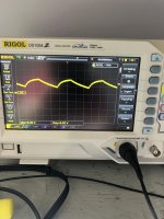
Load the PS FET locations (one at a time) with a capacitor between 0.1uf and 0.01uF (I use 0.047uF). Connect it between the gate and source pads. Check the waveform on the gate pad of the loaded FET.
The attached is the closest I likely have. All of the power supply components are hidden in the photo.
The attached is the closest I likely have. All of the power supply components are hidden in the photo.
Attachments
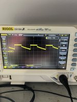
I dropped a 0.1uF cap in between the gate and the source. I measured the gate pad and before the gate resistor. I’m thinking all the transistors are likely not happy based on the readings I’m getting.
The pattern that looks more like a square is before the gate resistor. The pattern that looks more rounded is at the gate pad. When checking the rest of the drive transistors at the base pads, the pattern remain ok and the voltages all match.
The pattern that looks more like a square is before the gate resistor. The pattern that looks more rounded is at the gate pad. When checking the rest of the drive transistors at the base pads, the pattern remain ok and the voltages all match.