Hey all I'm wondering if anyone took some really good pictures of the schiit magnius circuit board. I've seen the one on their site and one other that is a little more zoomed in, but still at a high angle. I'm especially interested in what that cap is doing on the output of the tap6120a2 chips and also if they are using more or less the schematic in the data sheet or if they have done anything special. Especially with the opamp side of things.
I think the capacitor is there to isolate the line out (capacitor coupled; yellow arrows) from the (directly coupled; blue arrows) headphones outfeed.

... as for their TPA6120 Vcc and Vee pins' local decoupling technique... I am speechless.... unless they did it correctly on the underside.
Last edited:
but if you look one half of the output, what would be the left in each of the tap6120a2 chips (LOUT pin 2) is capacitor coupled, but the right channel (Rout pin 19) on each chip is not. Also that cap is huge. like really huge. it looks like 22-47uf when if I understand cap decoupling for audio correctly you'd be better off with 1uf. I've also been trying to learn from the topping a90 circuit and they have a high pass filter to ground, but no cap between the chip output and the connector. just from chip output, through a resistor, to ground.I think the capacitor is there to isolate the line out (capacitor coupled; yellow arrows) from the (directly coupled; blue arrows) headphones outfeed.
View attachment 1067888
actually looking at the pic again i guess 1 channel is cap coupled for the back output and the other channel is cap coupled for the headphone output? weird.
Attachments
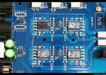
Yeah they must have caps on the underside. I know it's better to have them on the same side, but I've always heard the second best place for decoupling caps is directly under the chip through a via. The first being as close as physically possible on the same side, and least best is anywhere far away.... as for their TPA6120 Vcc and Vee pins' local decoupling technique... I am speechless.... unless they did it correctly on the underside.
Can't see any vias anywhere next to the Vee pins (blue)... which means that.... they couldn't do a proper decoupling on the underside... The Vcc vias are there just to feed the bus current to pins 3 & 18... from the vias next to C11, via the underside.Yeah they must have caps on the underside.
the vias might be under the chip. It's hard to say. like they could have extended the trace farther past the ic pinCan't see any vias anywhere next to the Vee pins (blue)... which means that.... they couldn't do a proper decoupling on the underside... The Vcc vias are there just to feed the bus current to pins 3 & 18... from the vias next to C11, via the underside.
View attachment 1068122
- Home
- Amplifiers
- Headphone Systems
- Better pictures of the schiit magnius circuit board?