Hello, I'm trying to learn about build little boards for some of my units that are messed up.
This boards are not that complicated compared with the usual ones that I see here, they are single side and usually semi burned, with broken pads and traces or several repair attempts.(hacks). These have been a hobby of mine from a while now and I have a ton of fun rebuilding them.
For that purpose I'm using easyeda, I find it easier to learn than KiCad or Eagle, but since I'm hook and kind of obsessed with this I'll learn them along the way.
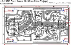
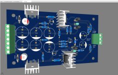
With that said, I made a first one, is for the power supply of my Sansui BA5000 and I wonder if you guys can point me if I'm in the right direction. Basically I made a ground plane on the bottom layer and else on top, but since I'm barely know what I'm doing be brutal, if my layout is useless I have no problem starting again with some pointers. That how I learn.
Cheers.
This boards are not that complicated compared with the usual ones that I see here, they are single side and usually semi burned, with broken pads and traces or several repair attempts.(hacks). These have been a hobby of mine from a while now and I have a ton of fun rebuilding them.
For that purpose I'm using easyeda, I find it easier to learn than KiCad or Eagle, but since I'm hook and kind of obsessed with this I'll learn them along the way.
With that said, I made a first one, is for the power supply of my Sansui BA5000 and I wonder if you guys can point me if I'm in the right direction. Basically I made a ground plane on the bottom layer and else on top, but since I'm barely know what I'm doing be brutal, if my layout is useless I have no problem starting again with some pointers. That how I learn.
Cheers.
Attachments
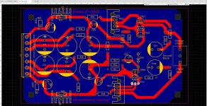
The only thing I can think of is if copper on the bottom wasnt part of the original board, you may be asking for trouble including it in your repro. It would show in some unanticipated anomaly that might be cause for a respin to remove it.

Good point.
I could make just one layer board on the bottom as in the 70's more in tune with the original design, it would make a nice practice as well, the well see if there is some difference.
Thanks!
I could make just one layer board on the bottom as in the 70's more in tune with the original design, it would make a nice practice as well, the well see if there is some difference.
Thanks!
I would clone the original board, period, not "improve" it.
If original was simple face + a couple jumpers, so be it.
Only advisable change would be small part size and pin separation adjustments, say original caps had 1/2" lead separation, modern ones have 10 mm, etc.
But nothing further.
If original was simple face + a couple jumpers, so be it.
Only advisable change would be small part size and pin separation adjustments, say original caps had 1/2" lead separation, modern ones have 10 mm, etc.
But nothing further.
Interesting topic - one thing I notice on the original board is the 2 white 'X' type shapes marked in the largest central trace area of the original pcb drawing (the Ground trace). What do these correspond to on the actual pcb? e.g., are there really 'X' shaped breaks in the trace area ? If so, why / what function do they serve ?
Make sure the ground plane of the new board does not connect to the chassis through the mounting screws/posts. If it does, you could be creating a ground loop that may cause noise or other problems. The original does not and the ground of this board is not necessarily at the same potential as the chassis ground.
Also, make sure the heat-sink solder posts do not connect to the ground plane otherwise you may be shorting the transistor or IC metal tab to ground and the circuit may not work at all unless you use insulating washers to mount the devices to the heat-sinks. The original heat-sinks are not grounded. Good luck.
Also, make sure the heat-sink solder posts do not connect to the ground plane otherwise you may be shorting the transistor or IC metal tab to ground and the circuit may not work at all unless you use insulating washers to mount the devices to the heat-sinks. The original heat-sinks are not grounded. Good luck.
Yes they do....That's a good question, mmmm I don't know.are there really 'X' shaped breaks in the trace area ? If so, why / what function do they serve ?
It is connected to the chassis by a wire to a star ground, but I understand what are you saying, I'll make a bigger clearence. Thanks!The original does not and the ground of this board is not necessarily at the same potential as the chassis ground.
Point taken, thanks!But nothing further.
Last edited:
With power supply boards, peak currents from the rectifiers can be high enough that the traces have to be considered as resistors. Changing the layout could increase ripple on the output voltages.
As for the Xs, maybe they're just there to reduce the heat sink effect of big areas of copper?
If I just needed one of those boards, and had that artwork and spare time... I'd print it out to exact scale, tape it to a piece of single-sided board stock, and drill all the holes. Scrub the copper clean, then cover it with packing tape. Then tape the artwork onto it, and cut along the trace outlines with a sharp knife. Peel away the packing tape where you want the copper gone, and float the board in your warm tray of etchant. (PC boards will float on ferric chloride etchant, and you can see the etched areas go dark when they're clear of copper. Just lower them slowly so there are no trapped air bubbles.)
The good old etching method!With power supply boards, peak currents from the rectifiers can be high enough that the traces have to be considered as resistors. Changing the layout could increase ripple on the output voltages.
As for the Xs, maybe they're just there to reduce the heat sink effect of big areas of copper?
If I just needed one of those boards, and had that artwork and spare time... I'd print it out to exact scale, tape it to a piece of single-sided board stock, and drill all the holes. Scrub the copper clean, then cover it with packing tape. Then tape the artwork onto it, and cut along the trace outlines with a sharp knife. Peel away the packing tape where you want the copper gone, and float the board in your warm tray of etchant. (PC boards will float on ferric chloride etchant, and you can see the etched areas go dark when they're clear of copper. Just lower them slowly so there are no trapped air bubbles.)
I already sent to print two versions of the boards, one with ground plane and one without it, both using two layers, with a some differences from the original board (not to mention parts) ... so we'll see once the testing is done if they perform or if the unanticipated anomalies cause a Gravitational singularity or something like that on my shop.
Cheers
- Home
- Design & Build
- Software Tools
- Learning to build boards for vintage equipment.