Dear community,
I am in a process of repairing my Sony TA-N9000ES amplifier. I am familiar with electronic, but my skills and experience with power amplifiers are very limited. I hope to receive some advices. A few words on how it failed.
It was a daily use amplifier. Just mid range volume, 8 ohms speakers. I noticed no sound coming out. Checked the amp, it is in protection mode, blinking LED. Turned it off with a power button, after a 20-30 seconds turned it back on and... enjoyed a fireworks with lots of smoke.
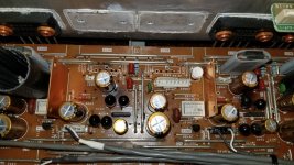
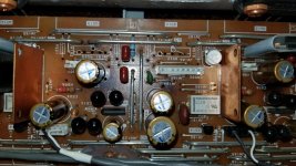
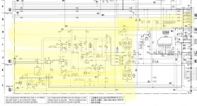
After opening it up and brief testing found positive voltage on center channel output. Static component testing showed that most of the components in this channel failed or evaporated, taking out some of the board traces. Did lots of cleaning.... ! First picture shows schematic with failed components in red circles. Second picture shows the worst burned area, in addition to a few more traces just disappeared.


I am in a process of repairing my Sony TA-N9000ES amplifier. I am familiar with electronic, but my skills and experience with power amplifiers are very limited. I hope to receive some advices. A few words on how it failed.
It was a daily use amplifier. Just mid range volume, 8 ohms speakers. I noticed no sound coming out. Checked the amp, it is in protection mode, blinking LED. Turned it off with a power button, after a 20-30 seconds turned it back on and... enjoyed a fireworks with lots of smoke.
After opening it up and brief testing found positive voltage on center channel output. Static component testing showed that most of the components in this channel failed or evaporated, taking out some of the board traces. Did lots of cleaning.... ! First picture shows schematic with failed components in red circles. Second picture shows the worst burned area, in addition to a few more traces just disappeared.

.22 ohm emitter twin resistors I could not find original - got similar. Power transistors and, just in case, Q501 I ordered from China and still waiting
 on delivery.
And now, before I receive the final stage transistors, I need help and advice on how to make sure that everything I have done is working properly. I am afraid to turn it on and see lots of fire again. Please suggest.
Thanks. Will do.
Can I test it for proper operation without the power transistors? and how to do it correctly?
Can I test it for proper operation without the power transistors? and how to do it correctly?
I appreciate your complimentIn any case, very nice repair work on the pcb ,it's nice to see . 👍
What would you think about doing something like that - disconnect the bios board, connect collectors Q508,515 and Q506,516 with the output to complete the feedback, and debug the channel with no output transistors. I am just brainstorming.

I am still interested if anyone can share an opinion on it.What is your opinion on doing something like that - disconnect the bias board, connect collectors Q508,515 and Q506,516 with the output to complete the feedback, and debug the channel with no output transistors. View attachment 1022402
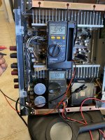
I have received all the parts ordered. Mounted output stage transistors, soldered in 2A fuses on B+ and B-. Double checked all elements and traces on the board. Used a bulb tester for start up. So far so good. Checked for bias in all channels on test pins - between 20 to 70 ma. Should be 11ma on 8 ohm load. Adjusted. Checked for DC offset - repaired channel 20 mv, all other between 1 to 5 mv. Definitely higher, however no adjustment on the board. Will concentrate on it.
Ended up replacing a differential pair Q501. The dc offset went down to 4.5 mv. Sounds way better. Now I have five channels with a dc offset between 0.5 to 4.5 mv. I would appreciate any opinions on that.
Can I modify an original design to implement a dc offset adjustment to get as close as possible to 0 v?
Can I modify an original design to implement a dc offset adjustment to get as close as possible to 0 v?
Hello,
nice work Hirurgi. I am trying to fix a 9000es as well. It got stuck on protection mode.
I did a visual check of the boards with a magnifying glass, unsoldered all the output transistors and checked with the dca75 pro tester and they all good. So I soldered them back and reflowed the all connectors, relays, some smd transistors and relays, man what a pita unit to work on my eyes got tired lol.
Someone else already replaced R220 and R221 on the protection section with right value but not fusible types so replaced them with fusible ones.
Fired it up with the dbt 100w bulb, and it dimmed quickly and the protection relay clicked and it works now.
I adjusted the bias to 8mv for all 5 channels. I checked the dc offset on all 5 4 were within 5mv or less, but the Front right one was at 104mv.
I tested all the resistors,
transistors (diode test method) and diodes on the FR section and pulled Q701 2SC5169, tested on dca75 the center pin is the common emitter btw, it tested good like HFE for both was within 1%. Anyways I swapped it the one from Q501, same thing dc offset read at 90mv. It’s still safe for use but I’d rather get the dc offset of FR close to zero.
any ideas on which components I need to check and test?
Attachments
Hello PineappleDave. 90 mv could be a little higher then desired. In my situation I have replaced every transistor and diode but Q507 - it tested good and it would not affect the dc offset. You mentioned that you tested all the resistors and continuity - done, swapped the diff pair - done. Testing transistors and diodes in diode test mode gives a good idea but they still could leak, and that will affect the dc offset. Faulty electrolytic capacitors could affect the dc offset too, in my opinion. At this point I would replace all the transistors, but power, and two diodes. They were very inexpensive to purchase and easy to replace. Swapping SMDs is a pain. Hopefully it will help. Please keep me posted.
To be exact I would start with Q702-703, next Q715,708, 706,716 and D704,702, lastly Q704,709. The very last stop got to be one of the power pairs.
- Home
- Amplifiers
- Solid State
- Sony TA-N9000ES Repair - Burned Channel