I appreciate that these are not exactly new devices, but I needed some complementary MOSFETs that would work well at 24v Vds and 10 mA Id and I could not find many choices. The application being for a headphone amplifier based loosely on the Sony VFET front end in case you are interested.
First problem was finding any N/P matches. Based on a relatively small sample (3 lots of 10 each from different suppliers) I obtained a range of Vgs values for the above conditions:
• 1.928 to 2.205v for ZVN3310A
• 3.351 to 3.510v for ZVP3310A
Not even close! Are my samples unusual or are these devices poor complements?
Just as a check I measured Vgs threshold (for 1ma Id) and obtained:
• 1.35v for ZVN3310A
• 2.0v for ZVP3310A
Consistent with the above results but less than ideal.
It also looks like the transconductance of the P part is rather less than that of the N by comparing the additional Vgs above the threshold required to reach 10 mA Id. However, I did not verify this as I don’t currently have a suitable test rig. The manufacturers datasheet is also of little help at these low currents. Long shot I know - but has anyone with a curve tracer measured these parts?
Finally, my devices exhibit a significant amount of self-heating at the desired operating point despite this being approx. 240mW when the device is supposed to be good for 625mW at an ambient temperature of 25C (close to the temperature here today). I guess the e-line package is rather small… So far I have tried introducing 221R source resistors but these appear too small to prevent Id from creeping slowly upwards. I suppose I shall have to increase the value but I don’t wish to go too far due to the associated voltage drop and hence reduced swing from the front end of the amplifier. Any suggestions?
I would prefer to stay with MOSFETs rather than introduce BJTs hence also interested in suggestions for suitable alternatives, preferably ones that are actually obtainable!
Hi Ian,
The ZVP3310 and ZVN3310 have been favorites of mine for a long time. I bought hundreds of each years ago. They don’t produce matches as easily as some of the To-220 pairs but I if you have enough parts you can do it. I don’t bother with P/N cross matches.
At 24 volts I limit the current to 3ma to 4ma for a dissipation of 100mw or maybe a bit more. I then parallel as many as I need to get the total current required. However, I still get some drift due to heating.
Graeme
to Ian Mcmillan
Hello Ian,
I've built a little preamp with the Zetex ZVN/ZVP3310 a few years ago.
I had similar problems like you. I had to measure a lot of the Zetex to get good matches. But it has a diffferential input. So only two devices per channel to be matched closely.
Recipe from whom? - Nelson Pass
Read this article:
https://www.firstwatt.com/pdf/art_diy_opamp.pdf
You will have to run pretty high railvoltages for a preamp.Sounds not bad...
The ZVP3310 was also used in the PEARL2 - phono-pre from Wayne Colburn. Very ESD-sensitive device!
Cheers
Dirk 😀
...the transconductance of the P part is rather less than that of the N...
This is universally true for FETs.
I thought I just saw it explained in Sze but can't find it today.
Conductance both as gain and as maximum current.
This is why "power" systems typically use only N-type. (At high voltages with strong drive chip it matters less.) It is why P-type power MOSFETs of Imax similar to an N-type cost more (bigger die). It is why P-type J-FETs are rare.
In CMOS the P-types are bigger than the Ns and even so there is asymmetry.
Let's not even consider the performance of P-type vacuum FETs.
Thanks for all the replies.
TN / TP2640 – look interesting although the input capacitance is perhaps a bit high. Still, worth further investigation.
So it seems that matching these devices N to P is generally hard if not impossible. Probably means I am going to experience rather more second harmonic than I would like. Time to look into some kit to measure this I think… BTW, I can manage reasonable N to N and P to P matches even with my small sample size.
Limiting the current to 4ma at 24v is going to be a bit of a pain given that I will need parallel pairs and I wish to eliminate source degeneration. Is this limit one that you have arrived at by testing or were you just playing safe Graeme?
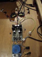
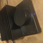
In the interest of sharing I’ve attached a picture of my headphone amplifier build.
TN / TP2640 – look interesting although the input capacitance is perhaps a bit high. Still, worth further investigation.
So it seems that matching these devices N to P is generally hard if not impossible. Probably means I am going to experience rather more second harmonic than I would like. Time to look into some kit to measure this I think… BTW, I can manage reasonable N to N and P to P matches even with my small sample size.
Limiting the current to 4ma at 24v is going to be a bit of a pain given that I will need parallel pairs and I wish to eliminate source degeneration. Is this limit one that you have arrived at by testing or were you just playing safe Graeme?
In the interest of sharing I’ve attached a picture of my headphone amplifier build.
Attachments
Ian,
For MOSFET’s other than laterals I limit power to 20% of the maximum allowable. This was a recommendation from Nelson in one of his articles. This has always worked for me. However I still run things for a couple of hours until the transistors heat up and establish thermal stability with ambient.
I recently built a circuit with three parallel pairs of these parts running 3.5ma per transistor at about 32v. Works fine. I will try to post a photo later today.
Graeme
These devices have fairly different Vgs specs to be true compliments. They can be made to work though.
Graeme – thanks for the 20% tip. I must have missed that particular piece of advice from Nelson. I too like to run things for at least an hour in order to reach thermal stability but of course that only works if there is no thermal runaway! I suspect I am seeing something like the latter in my ZVN / ZVP pairing since they just don’t seem to stabilise in any reasonable time.
Wayne: good to hear that these devices can be made to work. Are you prepared to offer any suggestions as to how or is that a secret?
Wayne: good to hear that these devices can be made to work. Are you prepared to offer any suggestions as to how or is that a secret?
Ian,
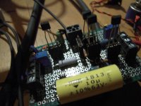
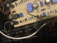
Here are the pics I promised. I am building a 200 to 250watt per channel balanced amplifier to drive a pair of mg3.6 speakers. It has a BA-2 output stage with 5 mosfets per quadrant. The front end will be from the Sony VFET project. However, I don’t have enough 2sk313/2013 parts, so I’m substituting paralleled 3310 mosfet pairs. The front end circuit you see in the picture is temporary and was used as a test bed. The next step is to build the VFET front end with the paralleled 3310’s, test that on the bench and then install it in the amp. Wish me luck.
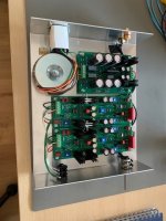
I included an ‘outside’ view of the overall amplifier. The power transformer is swag from BA 2008(?) and originally had a masking tape label that stated that it was pulled from an XA200 prototype shown at CES.
The amp as shown has been running successfully for 6 months. The 3310’s are not as thermally stable as I would like but they’ve behaved so far.
I hope this helps or encourages.
Graeme
Here are the pics I promised. I am building a 200 to 250watt per channel balanced amplifier to drive a pair of mg3.6 speakers. It has a BA-2 output stage with 5 mosfets per quadrant. The front end will be from the Sony VFET project. However, I don’t have enough 2sk313/2013 parts, so I’m substituting paralleled 3310 mosfet pairs. The front end circuit you see in the picture is temporary and was used as a test bed. The next step is to build the VFET front end with the paralleled 3310’s, test that on the bench and then install it in the amp. Wish me luck.
I included an ‘outside’ view of the overall amplifier. The power transformer is swag from BA 2008(?) and originally had a masking tape label that stated that it was pulled from an XA200 prototype shown at CES.
The amp as shown has been running successfully for 6 months. The 3310’s are not as thermally stable as I would like but they’ve behaved so far.
I hope this helps or encourages.
Graeme
Attachments
Hi Graeme
Thanks for the pics and indeed your general encouragement. Sounds like we are going down a similar route with the Sony VFET front end (FE) albeit for a different target – mine being for headphones. I didn’t adopt the parallel approach as I had hoped that a single pair would suffice for the relatively low current that I need. Seems I might well be wrong though.
I’m also making my life more complicated by trying to eliminate degeneration in both the FE and output stage to see if I can hear any difference. Probably I am guilty of trying too many different things at once.
I previously build the ACP headphone amplifier, modified to use a single JFET at the input. This sounded OK but not special with my fairly high impedance headphones hence trying a different approach this time.
Good luck with your VFET FE project though it sounds like you have things pretty well under control 🙂
Ian
- Home
- Amplifiers
- Pass Labs
- Any experience of ZVN3310 / ZVP3310?