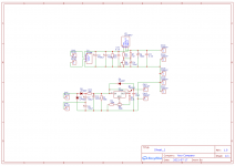
While I may never design my own circuits. I figured learning how to lay out a circuit board would be very useful for taking advantage of all the shared projects on this forum as well as reducing the cost of my builds. I've got a few tube preamp builds in mind. So I wanted to try an all in one regulated B+ and heater supply board. The heater supply is a copy of Pete Millet's low voltage regulator minus the CMC. And the B+ regulator is copied from the Antique Wireless World circuit based on the LR8N chip. Boards are available, of the individual circuits, from their respective designers. That being said I have no intention of sharing design files or boards. If, however, somebody is feeling generous with their time. I'd appreciate any feedback on my layout.
Attachments
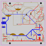
Thicker traces for any supply or gound line... You want low resistance and low inductance for these - often the latter is helped by using a ground-plane.
Thank you for the feedback. I see so many differing opinions on what trace thickness to use. What would you use for high voltage, low current and low voltage, high current? I'm going to rework the grounds to a bus for each supply instead of stringing components to each other as well
It costs less in manufacture to leave copper on.
It takes more chemicals to remove the copper.
It took me a couple of "mess ups" before I started to get pcb's right.
I designed a USB mixer.
Designed pcb without any thought for routing and when it came back and I shorted the input the output was 1VAC hum !
I had mixed in smoothing cap ground with audio ground.
So charging impulses into smoothing cap was modulating the ground line nicely !
Rerouted it keeping smoothing cap and audio ground separated and things were good.
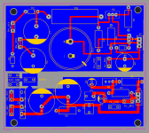
I did some more reading on layout. I see what you mean about "leaving the copper on." I made a little design change, changing the unnecessarily large film cap on the output of the B+ regulator to an electrolytic. And took another run at it. This time using large ground planes while still trying to keep the B+ and filament grounds from influencing each other.
Attachments
Remember you need "no copper" bare board between the pads/traces and the plane, roughly 3mm.
This is called creepage.
This is called creepage.
Last edited:
What power supply DC voltage are you using? If it's below 300V, then around 2mm
would be acceptable, but 3mm is fine regardless.
would be acceptable, but 3mm is fine regardless.
The preamp I'm currently looking at building is at 310V. Some others I'm considering are around that or lower. Max voltage for the regulator is 335V anyway. I'll go with 3mm just to be on the safe side
For the 300v supply I would use HER158G schottky rectifiers.
I used 1n4007 originally but got switching noise.
Alternative is a snubber across transformer secondary.
I used 1n4007 originally but got switching noise.
Alternative is a snubber across transformer secondary.
High voltage Schottkys are not very good, both leaky and fragile
UF4007 are fairly cheap and are quiet
UF4007 are fairly cheap and are quiet
It costs less in manufacture to leave copper on.
It takes more chemicals to remove the copper.
That depends, but these days if you order a bunch of PCB's it absolutely doesn't matter anymore at all. Just a fixed price for a certain quantity.
No matter if you keep it totally empty or not.
Same goes for vias and such.
The average manufacturing cost is baked into the cost to the end user.
Lower average mfr cost -> lower retail price. And less etching is better for the environment.
Lower average mfr cost -> lower retail price. And less etching is better for the environment.
Last edited:
Things have changed over the years, they used to charge for each via too at one time !
Same for 2 layers, often same price now.
PCB quality has gone up over the years.
In 1981 worked for a modem company.
The boss insisted on buying in cheap pcb's and half weren't fully etched.
So spent a fortune on me fixing them with a scalpel !
Of course half the track faults were beneath a soldered in IC !
That's not a Schottky rectifier, its an ultrafast standard Si diode.For the 300v supply I would use HER158G schottky rectifiers.
You'd never use silicon Schottky diodes for high voltage rectification due to the extreme risk of thermal runaway due to the reverse leakage current rising exponentially with temperature - you should heatsink Schottky rectifiers at even moderate voltages to prevent runaway.
Things have changed over the years, they used to charge for each via too at one time !
Same for 2 layers, often same price now.
PCB quality has gone up over the years.
In 1981 worked for a modem company.
The boss insisted on buying in cheap pcb's and half weren't fully etched.
So spent a fortune on me fixing them with a scalpel !
Of course half the track faults were beneath a soldered in IC !
Same for 2 layer?
In fact, depending were you order, but single layer boards can be even more costly those days. Just because almost no one uses them anymore
The default now is basically 4-layer.
Even in small quantities, the price difference compared to two layer is so small. Makes designing PCB much easier, quicker with a more robust design in general.
- Home
- Design & Build
- Software Tools
- 1st PCB design advice