If I make a real small PCB, mine is 1.25 inches by 2.5 inches and I order it with 2 oz copper and in addition my traces are wide (3mm) and I'm leaving both sides with their ground planes intact (all thru pads).
This being the case, I can pretty much consider thermal pads on opposite ends of such a small board to be "star grounded" correct? Since the copper is thick, traces are wide and the board is small and both sides have a plane left intact as much as possible.
But if I make a board that is 6 inches by 7 inches lets say, can I also consider thermal pads at opposite sides to be "star grounded"? Is there a point where a ground plane stops being somewhat of a star ground?
This is a small board to keep the transformer, bridge and first reservoir cap (two in parallel) in close proximity because every book I've read about power supply design says to keep that "trinity" on its own ground. Then bring the unsmoothed voltage to the filter train which then has its own separate star. This is presumably to keep the "dirty" first cap violent charging pulses in its own tight current loop.
This little board contains... Can I consider the 3 thermal pads on it to be effectively "star grounded" to each other?
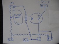
1) Secondary protection fuse
2) A "quasimodo" Cx,Cs,Rs snubber
3) A test point to determine the value of Rs needed using a "quasimodo" ringer before you install Rs
4) Four TO220 diodes in a bridge heat-sinkable to a small plate of aluminum off the long edge
5) Spaces for two 18mm radial caps in parallel (first reservoir) (using two in parallel to obtain an improved ESR over just one).
6) Board is 1.25 x 2.5 inches (32 x 64 mm).

This being the case, I can pretty much consider thermal pads on opposite ends of such a small board to be "star grounded" correct? Since the copper is thick, traces are wide and the board is small and both sides have a plane left intact as much as possible.
But if I make a board that is 6 inches by 7 inches lets say, can I also consider thermal pads at opposite sides to be "star grounded"? Is there a point where a ground plane stops being somewhat of a star ground?
This is a small board to keep the transformer, bridge and first reservoir cap (two in parallel) in close proximity because every book I've read about power supply design says to keep that "trinity" on its own ground. Then bring the unsmoothed voltage to the filter train which then has its own separate star. This is presumably to keep the "dirty" first cap violent charging pulses in its own tight current loop.
This little board contains... Can I consider the 3 thermal pads on it to be effectively "star grounded" to each other?
1) Secondary protection fuse
2) A "quasimodo" Cx,Cs,Rs snubber
3) A test point to determine the value of Rs needed using a "quasimodo" ringer before you install Rs
4) Four TO220 diodes in a bridge heat-sinkable to a small plate of aluminum off the long edge
5) Spaces for two 18mm radial caps in parallel (first reservoir) (using two in parallel to obtain an improved ESR over just one).
6) Board is 1.25 x 2.5 inches (32 x 64 mm).
There are too many cuts and obstructions for the plane to work very well.
Try reworking it with a nearly solid plane on one side, and most traces on the other side.
It might be easier if the board is a little larger. What is the large hole at bottom center for?
Try reworking it with a nearly solid plane on one side, and most traces on the other side.
It might be easier if the board is a little larger. What is the large hole at bottom center for?
Last edited:
There are too many cuts and obstructions for the plane to work very well.
Try reworking it with a nearly solid plane on one side, and most traces on the other side.
It might be easier if the board is a little larger. What is the large hole at bottom center for?
The bottom center hole is a thru pad that connects the A/K of the diode pairs left and right, the other A/K junction is right below it those were adjacent and easy. Physically I wanted all four diodes in line across a long edge, so I had to jump sides to get one of the two AK junctions to connect, that thru pad connects that jump across. As you know a bridge has two AK junctions for the AC, and a common K junction and a common A junction for the DC. There are only three traces I had to put on the other side out of all of them. The black rectangle is the actual outline of the board, I did a screen clip. The diode TO220 heat plates actually hang .25 mm over the edge of the board so you can bolt them onto aluminum without the board hitting the aluminum too.
Last edited:
I have a feeling that instead of 2 electrolytic caps in parallel, just one larger one in the center
would work out better. Then the snubber parts would be more at the top left, near the AC input.
And the fuse goes down the left side.
would work out better. Then the snubber parts would be more at the top left, near the AC input.
And the fuse goes down the left side.
Last edited:
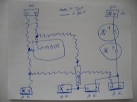
Ok, something more like this.
Lines are bottom traces, squiggles are top traces, X are to ground plane.
The upper end fuse trace could also be on the top.
Lines are bottom traces, squiggles are top traces, X are to ground plane.
The upper end fuse trace could also be on the top.
Attachments
Last edited:
Thanks for the drawing! I'll play around with it more I do want to keep two capacitors maybe just put them on one side and do the snubber like you have it. I do want it to be very small by design so it can be mounted under the transformer or on top of a toroid, then DC wired over to the filter train elsewhere, to physically separate it. I see what you mean a long trace along a side doesnt break the ground plane as much as going down the middle.
Last edited:
With two electrolytics, place them one above the other, with each cap's terminals on a horizontal line.
Keep the (-) terminals on the left side.
The trace to the top fuse terminal should best be on the top layer.
Try to keep the trace to the lower fuse terminal short to cut the plane less.
Move the fuse downward as much as possible, but it probably should remain vertical.
Ideally the fuse's lower terminal should be between the two diodes to which it connects.
Last edited:
OK here is my revision based on your advice rayma...
The goal was to keep one of the ground planes as un-broken as possible so those common anodes have a good current path. Here is top view and bottom view. I think I did ok here, the top plane is only broken by two short traces that need to get to the diodes. Cleaned up the snubber side, that didnt need wide traces these traces are more than the disc cap leads.
I put the reservoir caps next to each other, that will shorten their current path better than on opposite sides. The DC anodes now go directly to the plane but the plane is now uninterrupted and wide/thick. I still left the board as tiny as possible. Copper stops .5 mm from board edge all around. Leaving the bottom plane there even though its broken up with traces, just for more board rigidity.
Almost ready to order this, if no more tips, getting 2 oz copper on this order.
View from top (with X ray):

View from bottom (with X ray):

The goal was to keep one of the ground planes as un-broken as possible so those common anodes have a good current path. Here is top view and bottom view. I think I did ok here, the top plane is only broken by two short traces that need to get to the diodes. Cleaned up the snubber side, that didnt need wide traces these traces are more than the disc cap leads.
I put the reservoir caps next to each other, that will shorten their current path better than on opposite sides. The DC anodes now go directly to the plane but the plane is now uninterrupted and wide/thick. I still left the board as tiny as possible. Copper stops .5 mm from board edge all around. Leaving the bottom plane there even though its broken up with traces, just for more board rigidity.
Almost ready to order this, if no more tips, getting 2 oz copper on this order.
View from top (with X ray):
View from bottom (with X ray):
Looks much better. It helps when doing this to have designed a lot of single-sided boards,
which were common back in the "tape by hand" days (better forgotten).
which were common back in the "tape by hand" days (better forgotten).
Last edited:
Mounting with nylon hardware? You don't want to short the ground plane to whatever
the pcb is mounted on. Don't rely on the solder mask for insulation.
Where do you order from? Osh Park looks good for these small boards.
the pcb is mounted on. Don't rely on the solder mask for insulation.
Where do you order from? Osh Park looks good for these small boards.
Last edited:
I've been using jlcpcb, my last order they charged me $2 for 5 boards 1 oz. It was my 6th order with them, the first 5 were not as cheap as that, cheap, but $2 is ridiculous. I think they reduce the pricing after your 5th order. I left 1.5 mm around the mounting holes, I may up that to 2 mm. This will be 2 oz copper so price will be higher. I'm waiting for a bag of fuse clips to come so I get that spacing right, then Ill order it. I like to print the board then stab parts through the paper to make double sure drillings are right first too.
Good idea, it's hard to be too meticulous when checking a pcb.
It's very hard to get everything right on the first version.
Do verify the hole sizes also.
It's very hard to get everything right on the first version.
Do verify the hole sizes also.
Mirror image the board and parts with a central ground pont down the middle.
That's the way I do it, and never have a problem.
That's the way I do it, and never have a problem.
This is the bridge version. I want to make a half wave version too. Ironically that will be a slightly larger board even though it has only two diodes. Because the Quasimodo snubber has to be done twice, each side of the CT.
Star ground works by excluding error currents from the ground returns of sensitive signals completely, so that IR voltages aren't superimposed on the sensitive signals.
Groundplanes work by reducing resistances (1oz copper has a resistance of 0.5 milliohms-per-square(*), so even an amp only generates 500uV or so).
Solid groundplanes are mandatory for RF, where gaps and slots act as radiators and stray capacitance is much more important - its a nice simple solution for many situations, but for best audio performance careful star-grounding can be much better - prevention is better than dilution.
However you also have to worry about induction and keeping high current loops small in area - and also sensitive input circuits small in area too. And groundplanes interact with loop currents above them too - its complicated - especially at the higher audio frequencies where stray capacitance and inductance become more significant - star-grounding can't deal with these.
(*) Areal resistivity of a sheet conductor is scale-independent - just like stacking 4 resistors 2P2S gives the same value as each individual resistor.
It is all about ground loops.
Tying All points to a single star ground will not eliminate ground loops.
Problematic ground loops:
B+ ground loops:
B+ rectifiers / bridges / center tapped or not / must connect Directly to the first (and sometimes second filter caps; before connecting from there to the central / star / ground point. Keep that loop local.
Input signal ground loops:
RCA input jack return lead needs to be returned Directly to the bottom of the cathode circuit that would be returned to ground (cathode, self bias network resistor, feedback resistor, etc.). Keep that loop local, before connecting it to the central / star ground.
Some other circuit returns may also require a Direct Local Loop connection, before they are connected to the central / star ground.
Ground loop control (local loops).
Good filtering of B+ is also paramount.
Proper space and proper angular orientation of magnetics is also paramount (power transformers, chokes, interstage transformers, output transformers)
Attention to details pays off.
Most of my amplifiers have less than 100uV of hum and noise at the speaker output terminals (less than 0.1mV).
When you get the hum and noise that low, you either had good luck, or you did all the things right.
Good enough for my speakers, but not good enough for many Headphones.
Last edited:
Simplest solution is go to 1 oz copper, 4 layers and tie the 2 center layers as ground planes. That size from JLCPCB will be very inexpensive.
G²
G²
Simplest solution is go to 1 oz copper, 4 layers and tie the 2 center layers as ground planes. That size from JLCPCB will be very inexpensive.
G²
Cool, and I could learn how to do my first 4 layer board!
- Home
- Amplifiers
- Tubes / Valves
- At what point is a ground plane no longer a star ground?