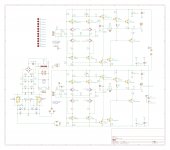
I tried my best to make this circuit as small as possible, did I position things too close together? Also can someone double check, that in general, I routed everything right. I'm a newbie, this is only the second board that I have sent to a PCB house and the first one I didn't design right.
Attachments

Adjust your page settings in the scheme editor to make the page big enough for your entire design.
Also, try to give space from the scheme symbol to the junction. I know that you can get a junction right on the part, but it's nice to have a little space for that. I cannot see any ground symbols in your design either. Resize your page and get us a new image to see better.
S
Also, try to give space from the scheme symbol to the junction. I know that you can get a junction right on the part, but it's nice to have a little space for that. I cannot see any ground symbols in your design either. Resize your page and get us a new image to see better.
S
Adjust your page settings in the scheme editor to make the page big enough for your entire design.
Also, try to give space from the scheme symbol to the junction. I know that you can get a junction right on the part, but it's nice to have a little space for that. I cannot see any ground symbols in your design either. Resize your page and get us a new image to see better.
S
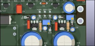
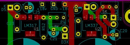
Thank you for the quick response and constructive criticism, I moved things around a bit to make it easier to read and edited the page settings to fit the whole schematic. I am open to any and all suggestions.