Good morning.
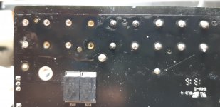
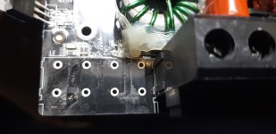
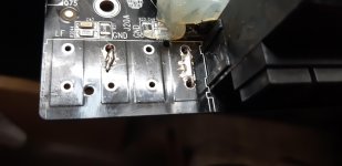
I have this RF punch 1000x5 here. Front right channel had no output. Problem appears that the vias both broke off on the Right neg. And one from the left neg.
I think I can still get the left neg to connect reliably.
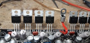
Question is... best way to connect the right neg. Can I just run a straight wire to the drain of the IRF3415? Is there a better way?
Thanks in advance
I have this RF punch 1000x5 here. Front right channel had no output. Problem appears that the vias both broke off on the Right neg. And one from the left neg.
I think I can still get the left neg to connect reliably.
Question is... best way to connect the right neg. Can I just run a straight wire to the drain of the IRF3415? Is there a better way?
Thanks in advance
Attachments
Last edited:
If you know where the leg should be connected to, you can solder a wire in between (that is basically what the standard copper traces are as well).
Or if you can see the trace, just follow the trace, or connect a wire to the trace.
I think you pulled the vias out when desoldering. I think it is reliable enough to just scratch a bit of the original trace, and solder some clean copper wires (from about 1cm or so) between the trace and the pin.
If you want to be sure, solder a wire in between
I'd scrape the soldermask from the top of the board. Solder a small wire to the bare copper and pass it (one continuous wire) through the vias. If you apply plenty of flux and tin the terminals well, the solder should flow into the vias and fill, even without the pad. If nothing else, the terminals will solder to the wire.
If you know where the leg should be connected to, you can solder a wire in between (that is basically what the standard copper traces are as well).
Or if you can see the trace, just follow the trace, or connect a wire to the trace.
I think you pulled the vias out when desoldering. I think it is reliable enough to just scratch a bit of the original trace, and solder some clean copper wires (from about 1cm or so) between the trace and the pin.
If you want to be sure, solder a wire in between
The vias and pads were damaged by over tightening the terminals. The whole solder connection to the pad was broken from the vias. I could wiggle the whole connection around in the holes before I touched it at all. I used chipquick to try and salvage anything I could of it. I didn't damage anything.
I'm not sure if this is a 3 layer PCB... but tracing the trace from the top seams impossible... and there is no connection to the bottom.
I'll try jumping wire from top into the via holes. Thanks
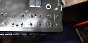
You have to be careful when drilling boards that may be more than 2 layers. It's possible that you could break an internal connection.
- Home
- General Interest
- Car Audio
- Best way to repair?