The Mark Levinson 23 and 23.5 are great amps, but given their age of almost 40 years, it is no surprise that quite a number of them are starting to suffer from all kinds of minor problems up to fully blown output stages.
Since this amp was never designed for easy repair, it is quite a challenge to take boards apart without damaging the aged PCB.
That's why, after having repaired a number of them, I was thinking of producing a whole new PCB with modernised circuits, but still largely based on the Mark Levinson DNA.
All bipolars on the heatsinks are supposed to be reused with the new design, based on a high quality PCB with all basic control functions like regulated power supply and protection circuitry.
On top of this baseboard a socketed module is thought with the amplifier module minus OPS.
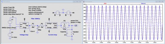
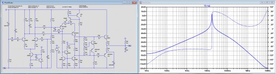
So far I have designed all modules in LTspice: regulated Jung-Didden power supplies, start up circuitry, output protection circuitry making boards OL-2 obsolete, etc. etc.
All modules are put in sub circuits, to get an easy model for the coplete amp in LTSpice.
However with all those subcircuits, LTSpice gets very slow, that's why I replaced a number of opamps with the generic opamp2, set with the correct parameters.
I have of course tested all individual modules separately to prevent that results deviate from the real opamps to be used.
What I haven't included in the model below are the regulated power supplies and the output protection circuitry, to keep simulation time at an acceptable level.
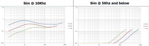
In the images below, you see a full 800Watt sim into a 2R load.
Distortion from the first stage as shown is 0.2 ppm with an overall distortion at the LS of 2.6 ppm.
Of course these figures are on the bright side, but definitely not more than a factor 10 off.
I'm just looking for some feedback to decide whether to go on with this project or not.
If you want to give the sim a try, the main .asc is below and unzip the file with subcircuits and libraries into the same directory.
Hans
Since this amp was never designed for easy repair, it is quite a challenge to take boards apart without damaging the aged PCB.
That's why, after having repaired a number of them, I was thinking of producing a whole new PCB with modernised circuits, but still largely based on the Mark Levinson DNA.
All bipolars on the heatsinks are supposed to be reused with the new design, based on a high quality PCB with all basic control functions like regulated power supply and protection circuitry.
On top of this baseboard a socketed module is thought with the amplifier module minus OPS.
So far I have designed all modules in LTspice: regulated Jung-Didden power supplies, start up circuitry, output protection circuitry making boards OL-2 obsolete, etc. etc.
All modules are put in sub circuits, to get an easy model for the coplete amp in LTSpice.
However with all those subcircuits, LTSpice gets very slow, that's why I replaced a number of opamps with the generic opamp2, set with the correct parameters.
I have of course tested all individual modules separately to prevent that results deviate from the real opamps to be used.
What I haven't included in the model below are the regulated power supplies and the output protection circuitry, to keep simulation time at an acceptable level.
In the images below, you see a full 800Watt sim into a 2R load.
Distortion from the first stage as shown is 0.2 ppm with an overall distortion at the LS of 2.6 ppm.
Of course these figures are on the bright side, but definitely not more than a factor 10 off.
I'm just looking for some feedback to decide whether to go on with this project or not.
If you want to give the sim a try, the main .asc is below and unzip the file with subcircuits and libraries into the same directory.
Hans
Attachments
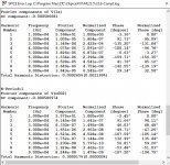
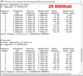
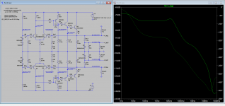
The shown distortion figures in the above posting where a bit fuzzy because the distortion between brackets behind the shown figures were completely different.
That's why I redid the sim, but now with a time window 5 times as long.
Strange values in brackets have now gone, but the original values for V(Ls) and V(n002) are still the same.
V(n002) as the second distortion value is for the signal after the first order 300kHz filter before entering the Current Amp.
Now added in a graph are the distortion figures in ppm for resp. 2R, 4R and 8R LS Load from 1.5Watt up to the maximum with 40Vrms.
Same caution as before that these figure are "on the bright side", but it's hard to improve on these fabulous low THD figures.
Hans
.
Attachments

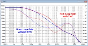
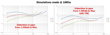
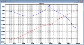
I went on trying to improve THD a bit further, not as a necessity because already very low, but just as a challenge.
The main THD production at 10Khz came from the OPS with it's double nested feedback.
By applying TMC to the inner feedback loop, I could improve THD @10Khz on average by more than 10dB without sacrificing on stability or any other negative effect that I could find.
However after also applying TMC to the outer feedback loop, although THD went down by another 10dB, settling time when applying a square wave increased by a factor >10, showing a signal slowly creeping to its final value.
That's why I rejected this option.
THD graphs for the complete amp @10Khz without and with TMC are shown in the first image.
The second image shows the overall THD for 10Khz and 5Khz next to each other, both with TMC.
Third image shows the loop gain for both versions without and with TMC.
Simulations with TMC are showing a THD below 1ppm for loads from 2R to 8R, power outputs up to 800Watt and all audio frequencies.
Below 5Khz, THD from the OPS was in all cases below the THD from the IPS.
The IPS could also have been improved with TMC, but that seems beyond making any sense.
So this as low as I like to go for a complete new 23.6 while using 100% of the existing OPS from the Mark Levinson 23.x
Hans
.
Attachments
Last edited:
Hi Victor
So do I, but as with all things in life somewhere it ends.
This project started with the idea to give this excellent amp a true life extension.
Hans
So do I, but as with all things in life somewhere it ends.
This project started with the idea to give this excellent amp a true life extension.
Hans
Go Hans! Go Hans! Go!
I will definitely order PCBs for my 23.
What component size are you thinking on the PCB?
I will definitely order PCBs for my 23.
What component size are you thinking on the PCB?
Even I was able to run AC analysis with the LTSpice!
Balanced input and all, nice.
It would be interesting to have impedance curve of my speakers measured and added in the output if it makes a difference.
Balanced input and all, nice.
It would be interesting to have impedance curve of my speakers measured and added in the output if it makes a difference.
As you mentioned the voltage regulator is completely new. I do not see 117V pre regs and 12V buffer voltages. Can you open that a bit, Hans?
Go Hans! Go Hans! Go!
I will definitely order PCBs for my 23.
What component size are you thinking on the PCB?
Hannu,
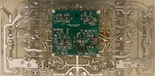
This picture below gives you an impression.
A large bottom board with the size of the current ML23.X PCB will connect to the transistors on the heatsinks.
The only additional functions that are planned on this large PCB are the two regulated supplies for Vreg+ and Vreg-
All other functions, including the external OL-2 board, will be located on this socketed green PCB that's on top.
On the lower halve of this board is the IPS or voltage amplifier.
In the left above corner the double nested feedback circuitry for the Current amp or OPS.
At the upper right corner you see the circuitry for all protection and start up functions.
The shown amplifier board is the PCB that I made for the ML20.x, but for the ML23.X this board will be for 98% the same.
When having a socketed amplifier board, testing will be much easier, that's the idea behind it.
Hans
Attachments
Nice!
So all the transistors that are now connected to the big heatsinks will be there with the new bigger board too?
I have noticed that the 4 transistors(VAS stage?) Q23,Q25,Q28,Q26 that are connected individual heatsinks are running crazy hot so maybe it would be good idea to increase cooling there. But on the other hand they have been working like that for over 30years and not broken, at least for me so why change...
As you mentioned the voltage regulator is completely new. I do not see 117V pre regs and 12V buffer voltages. Can you open that a bit, Hans?
Here is the positive regulator together with it's ripple rejection.
Compare this to the ML23.x version and even the ML336 one to see how much better this is.
Hans
Attachments
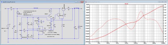

You did it right, but you already used the modified version with a 27R instead of 2.2R emitter resistor for the MJE output transistor.
Below is the PSRR of the original version in blue together with the newly developed one in red.
Up to a few hundred Khz, PSRR for the new version is at least 60dB better.
Hans
Below is the PSRR of the original version in blue together with the newly developed one in red.
Up to a few hundred Khz, PSRR for the new version is at least 60dB better.
Hans
Attachments
That is awesome, Hans! I forgot that resistor.
And for Victor, If you have the original ML23 and if you want to have these PCBs from Hans, You will get first of all all the modifications that are in ML23.5 + extras that Hans is making(like this new voltage regulator).
I am pretty sure that the sound will be a few steps better.
And for Victor, If you have the original ML23 and if you want to have these PCBs from Hans, You will get first of all all the modifications that are in ML23.5 + extras that Hans is making(like this new voltage regulator).
I am pretty sure that the sound will be a few steps better.
Hello Hannu,
I had a large project that came in between that delayed my attempts to come with a solution, but that project was finished last week.
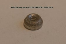
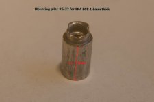
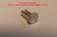
The circuit diagrams are ready and tested, but I have a problem in locating the following parts, see images. These parts are important to guarantee compatibility.
Maybe someone can help.
Hans
I had a large project that came in between that delayed my attempts to come with a solution, but that project was finished last week.
The circuit diagrams are ready and tested, but I have a problem in locating the following parts, see images. These parts are important to guarantee compatibility.
Maybe someone can help.
Hans
Attachments
Thanks for the update, Hans.
The last picture have to be the input connector pin for the input signal from the OL-2 board. Can that just be left away because we anyway need to solder the cable to the pin(or board)?
Or use other connector type perhaps? I can imagine that these are very hard to find.
The last picture have to be the input connector pin for the input signal from the OL-2 board. Can that just be left away because we anyway need to solder the cable to the pin(or board)?
Or use other connector type perhaps? I can imagine that these are very hard to find.
True. The input connector has the lowest prority.
The problem however is that the PCB is separated from the heatsinks by some thin plastic foil.
When using an input connector that is sharp on the solder side, it could puncture the plastic and contact the grounded heatsink.
But with TLC after soldering that can be taken care of.
The two other parts are very vital.
Hans
Hans,
if you're intending to sell your replacement boards to happy ML owners, might it be an option to apply metric parts and add the requested (metric) screws?
Best regards!
if you're intending to sell your replacement boards to happy ML owners, might it be an option to apply metric parts and add the requested (metric) screws?
Best regards!
Hi Kay,
Very good suggestion, but I've spent already a lot of time finding an optional M3.0 or M3.5 replacement with no results so far.
Larger sizes are readily available but this size is a real problem.
Seems as if ML had them produced on their proprietary specifications.
If not solved, this is a real deal breaker.
Hans
- Home
- Amplifiers
- Solid State
- Upgraded PCB for ML23.5