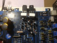
Small 2 channel class B assian amp.
Does not have any output but powers up fine and draws 0.3A at idle. I do not have any schematic on this one.
Rail voltages are fine, +-15v are dead stable.
No shorted diodes or transistors. Both channels are acting identical, so this should be a general issue, not channel related. I will be referring to only one of the channels for simplicity.
I've read everything in Perry's guide about amplifier stages.
I've narrowed down the issue somewhere in differential amp or/and voltage amplifier.
The voltage amplifier does not have any output - ( uses A1268 + C3200). There is +-22v at both emitter and base, and 0v the collector so it's not driving the output stage.
Base of the VAS transistors are directly connected to the collector of the differential amps - (uses A1015 + C1815). This amp uses constant current source for the differential amp stage.
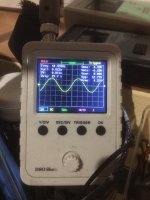
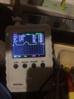
On the bases of the differential amp transistors I have a nice clean sinewave of 40hz - this is the input.
Collectors are purely DC - +-22v (from the guide i know i can't see here any sinewave but this should be driving the VAS).
Emitters have half sinewave sitting at them - one differential amp is having only top, the other one only the bottom part of the sinewave ground referenced.
I can't wrap my head around this. There are no shorted transistor or diodes, traces are fine, didn't find any bad resistor and both channels are acting identically...so what is affecting both channels and can cause this ?
There is an optocoupler 817c, but I've already changed it and no difference.
Any ideas ?
Does not have any output but powers up fine and draws 0.3A at idle. I do not have any schematic on this one.
Rail voltages are fine, +-15v are dead stable.
No shorted diodes or transistors. Both channels are acting identical, so this should be a general issue, not channel related. I will be referring to only one of the channels for simplicity.
I've read everything in Perry's guide about amplifier stages.
I've narrowed down the issue somewhere in differential amp or/and voltage amplifier.
The voltage amplifier does not have any output - ( uses A1268 + C3200). There is +-22v at both emitter and base, and 0v the collector so it's not driving the output stage.
Base of the VAS transistors are directly connected to the collector of the differential amps - (uses A1015 + C1815). This amp uses constant current source for the differential amp stage.
On the bases of the differential amp transistors I have a nice clean sinewave of 40hz - this is the input.
Collectors are purely DC - +-22v (from the guide i know i can't see here any sinewave but this should be driving the VAS).
Emitters have half sinewave sitting at them - one differential amp is having only top, the other one only the bottom part of the sinewave ground referenced.
I can't wrap my head around this. There are no shorted transistor or diodes, traces are fine, didn't find any bad resistor and both channels are acting identically...so what is affecting both channels and can cause this ?
There is an optocoupler 817c, but I've already changed it and no difference.
Any ideas ?
Attachments

Last edited:
Sometimes one may need to be bite the bullet and start sketching up a schematic by following/ringing-out traces.
Is the CCS passing current?
Are the emitters of the positive diff amp transistors 1/2v below the bases?
Are the emitters of the negative diff amp transistors 1/2v above the bases?
0v on the collectors? Are you sure? That would mean that the collector in each channel drive the speaker terminal. Is that correct?
Are the emitters of the positive diff amp transistors 1/2v below the bases?
Are the emitters of the negative diff amp transistors 1/2v above the bases?
0v on the collectors? Are you sure? That would mean that the collector in each channel drive the speaker terminal. Is that correct?
Is the CCS passing current? - the emitter resistor of the differential amp shows up 0.00 voltage across. So there is no voltage drop - no current draw.
Are the emitters of the positive diff amp transistors 1/2v below the bases? - they actually are above by 0.63v
Are the emitters of the negative diff amp transistors 1/2v above the bases? - they are bellow by 0.48v
0v on the collectors? Are you sure? That would mean that the collector in each channel drive the speaker terminal. Is that correct? - no, it's emitter driven.
I've attached a similar schematic. It's not exactly the same, but pretty close.
Differential amp transistors emitters should receive the opposite voltage in reference to their collector voltage, should not they ? If +30v are present at their collector, there should be MINUS 0.6v on the emitter ? 😕
Attachments

Last edited:
For the schematic posted, it looks like the points marked c1815 and a1015 might be the collectors of current sources (perhaps powered from the opposing rails) that allow each input differential pair emitters to float up and down.
It would be helpful to see some more voltage and current data around the input stage. Emitter resistor voltage drops can be used to calculate currents.
It would be helpful to see some more voltage and current data around the input stage. Emitter resistor voltage drops can be used to calculate currents.
Last edited:
This is for the one of the channel and one of the differential amplifiers. The schematic is the same for the the other part with opposite voltages, c3200 instead of a1266 and a1015 instead of c1815.
Sorry for my bad drawings, but this is actually the first schematic i've ever drawn in my life 😀
Hope that helps a bit more
Measurement were made with reference to the secondary GND (center tap). No RCA plugged in.
Sorry for my bad drawings, but this is actually the first schematic i've ever drawn in my life 😀
Hope that helps a bit more
Measurement were made with reference to the secondary GND (center tap). No RCA plugged in.
Attachments

Last edited:
The bases of the differential stage transistors are biased to 0v. Their emitters connect to a voltage source opposite that of their collectors but it's through a voltage dropping resistor.
For one channel, what's the resistance between the collectors of the two output transistors?
What's the resistance between their emitters?
One of the regulator filter caps next to one of the Zener diodes looks like it vented. Was there a problem in that area?
For one channel, what's the resistance between the collectors of the two output transistors?
What's the resistance between their emitters?
One of the regulator filter caps next to one of the Zener diodes looks like it vented. Was there a problem in that area?
So why then the voltage on their emitters is the same "charge" as on their collectors ?
Output BJTs.
Between collectors - megaohm range
Between emitters - 0.1ohm (this is the lowest my DMM can read)
I've changed that cap since the pictures were taken, but no change.
Output BJTs.
Between collectors - megaohm range
Between emitters - 0.1ohm (this is the lowest my DMM can read)
I've changed that cap since the pictures were taken, but no change.
In the tutorial, go to the Power supply troubleshooting page (PSTS in the quick links), item #33, then example 5. Does that look like what you have?
Is the equivalent of C601 electrically leaky?
Is the equivalent of C601 electrically leaky?
Sorry for my bad drawings, but this is actually the first schematic i've ever drawn in my life 😀
Looks an error in drawing the schematic. One transistor is shown with a capacitor in series with the base. A transistor needs to be biased on, and that won't happen if no DC path to the base exists. Right?
That's okay, it can take some practice to sketch up circuits and analyze them. I would suggest spending some more time on it to make sure you have it right.
Do you understand how all the circuitry that you sketched is supposed to work together? A current source, some degeneration resistors on the emitters of a differential pair, etc.?
Last edited:
In the tutorial, go to the Power supply troubleshooting page (PSTS in the quick links), item #33, then example 5. Does that look like what you have?
Is the equivalent of C601 electrically leaky?
I've re-capped the whole bloody thing. No change.
Actually my amp is almost identical to the one in example five. The resistors values are a little bit different, the transistors are not exactly the same, but the schematic is 1:1.
I've made the corrections, pictures attached. Present voltages are in red.
Diodes reads fine with the DMM but there is no voltage drop across them ? Leaky ? But all 8 of them, that gonna be 1 in million chance.😕
Attachments


Linen89,
The reason you have almost the same voltage on both sides of the diodes at Q509 is because almost no current is flowing. With little or no current there can be no voltage drop. Its just Ohms Law.
Unless there is more circuitry attached to the nodes labeled +15v and +13.6v, it probably means PC817 output is not turned on. That looks like the only path that could draw enough current through the diodes to bias them more fully on. Does that explanation make sense?
Yeah that's all clear.
Still can't figure out why the heck this amp is not working.
PC817 output is not turned on - if there is 14.4v on the anode and 13.8v on the cathode doesn't that state the optocoupler is working ? There is exactly 0.6v of voltage drop across it as expected.
The only thing that's attached to the +-15v is the pre-amp, but this one works perfectly fine.
Optocoupler inputs are LEDs. How much voltage does a LED drop? 1.2v? 1.8v?
Well, you have 14.4v minus 13.8v equals 0.6v, which is not enough drop for an LED. That makes sense?
As you can see this stuff isn't really too hard. A little simple arithmetic and Ohms Law can get you a lot of progress.
Well, you have 14.4v minus 13.8v equals 0.6v, which is not enough drop for an LED. That makes sense?
As you can see this stuff isn't really too hard. A little simple arithmetic and Ohms Law can get you a lot of progress.
I got confused by the anode / cathode thinking it would be more like a regular diode with a voltage drop of 0.6-0.7v.
As you can see this stuff isn't really too hard. A little simple arithmetic and Ohms Law can get you a lot of progress - this totally true
As you can see this stuff isn't really too hard. A little simple arithmetic and Ohms Law can get you a lot of progress - this totally true
When measuring the voltage on an opto-coupler, it's generally best to measure directly across the terminals of each half of it, at least initially.
What's the DC voltage directly across terminals 1 and 2?
Across 3 and 4?
What happens if you use your meter probe to short 3 and 4 together? Does the amp produce clean audio?
What's the DC voltage directly across terminals 1 and 2?
Across 3 and 4?
What happens if you use your meter probe to short 3 and 4 together? Does the amp produce clean audio?
Measuring across:
Terminal 1 and 2 = 0.25v
Terminal 3 and 4 = +-30v depends on probe orientation
Yes, shorting terminal 3 and 4 produces clean audio at both channels.
Terminal 1 and 2 = 0.25v
Terminal 3 and 4 = +-30v depends on probe orientation
Yes, shorting terminal 3 and 4 produces clean audio at both channels.
Okay. The problem appears to be before the optocoupler. What circuitry connects to pins 1 and 2?


Mother of all Gods...I've just fixed it...It's incredible how much additional information You can learn while troubleshooting an issue which can be so simple.
It was R601 in the schematics. It was open, but i could not measured it correctly while in the board and the diode next to it was skewing my readings. So i've had to lift one of the legs of the resistor in order to get correct readings. There were no any signs of heat or whatsoever.
I guess just a random component failure ?
Thank You all, this was really helpful and I've learnt a lot about differential and voltage amplifiers (The guide is incredibly helpful Perry).
- Home
- General Interest
- Car Audio
- differential amp issues