Hi guys,
I am studying the three stage amp topology. I understand why the voltages are set the way they are when there is no feedback loop.
However, I would like to understand why introducing the feedback sets the VAS's collector voltage somewhat below 0 as we need it to be instead of close to the negative rail.
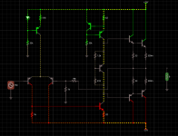
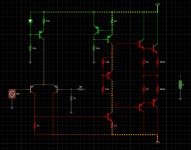
This is Bob Cordell's circuit which I modeled to better visualize it.
I appreciate your help,
thank you
I am studying the three stage amp topology. I understand why the voltages are set the way they are when there is no feedback loop.
However, I would like to understand why introducing the feedback sets the VAS's collector voltage somewhat below 0 as we need it to be instead of close to the negative rail.
This is Bob Cordell's circuit which I modeled to better visualize it.
I appreciate your help,
thank you
Attachments
Last edited:
You have a VBE multiplier providing the bias. The voltage across the emitter-collector of the VBE multiplier is centred about 0V for proper operation. This means, the collector voltage has to go slightly negative. The opposite applies to the emitter.
A VBE multiplier supplies a voltage a few multiples of 0.65V. It can never reach the negative rail voltage, that would be too much for a VBE multiplier.
A VBE multiplier supplies a voltage a few multiples of 0.65V. It can never reach the negative rail voltage, that would be too much for a VBE multiplier.
Last edited:
Thank you for your answer edbarx,
When there is no feedback you can see that the current source's transistor takes the big rail to rail voltage difference, and as i see it,it's collector voltage is controlled by the VAS's collector voltage plus the multiplier's VCE.
The multiplier sets a voltage difference of about 1.2V between the NPN and the PNP bases. This happens in both situations.
But why is the VAS's collector voltage changing so much when the feedback is connected?
The non-inverting input is usually pulled down to 0V with a resistor. The inverting input has to seek the same voltage, in this case 0V, to keep the voltage difference between the inputs as small as possible. The inverting input is driven by the output through a feedback chain resistor. To do this, the VAS is driven to keep the VBE multiplier's voltages near 0V to provide the correct base drive for the output to seek 0V.
Are you testing this with no load? If you do, and without feedback, you probably see the output floating to some undefined output DC, depending on the particular currents in the Vas stage. Remember, the Vas output voltage is not defined and depends on the currents into and out of that stage. The top current source and the bottom current from the LTP will not be exactly the same. You need the (DC) feedback to balance the input pair so that it matched the Vas CS on top.
With a load it may be better but still you'd see a large DC offset.
With feedback, the the two inputs will be very nearly equal, and the output will be driven to whatever is needed for that, and the Vas will be driven to whatever is needed for that.
For truly very low offset, use a series resistor in the signal input which is the same as the feedback impedance, to cancel the effect of the two DC currents into the bases of the input transistors.
Jan
Last edited: