I am working on building a stereo amplifier using the C300 amplifier of Michael Chua of Ampslab. It is a Class AB BJT-based stereo amplifier capable of 300 watts per channel. I have the PCB's on my github at
GitHub - profdc9/PowerAmpAudio: Power Amplifier based on Michael Chua's C300 amplifier
You can read about the C300 at
https://ampslab.com/c300.htm
c200 Power Amplifier @ AmpsLab
There are four PCBs in the project so far:
1. C300 amplifier PCB
2. Power supply rectifier and filter (low pass filters and common-mode chokes)
3. Soft start PCB for toroidal transformer and capacitor bank based on DIY audio's soft start
4. Balanced XLR to unbalanced input for the amplifier (based on THAT1200 / THAT1240 / SSM2141).
The schematics and gerbers are all there as well as BOMs with component part numbers mostly from LCSC.com , with a few digikey and Mouser parts as well. I release my projects under the Creative Commons license. The PCBs can be made at PCB factory like JLCPCB or PCBWay; I am using JLCPCB.
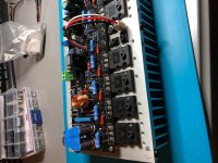
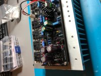
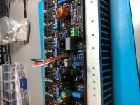
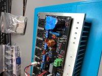
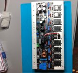
We have ordered all of the stuff and are going to photodocument the build. As an example I have a screenshot of the PCB. Check out the archive. I also have other many projects I have created on my github (but mostly not audio equipment related).
Dan
GitHub - profdc9/PowerAmpAudio: Power Amplifier based on Michael Chua's C300 amplifier
You can read about the C300 at
https://ampslab.com/c300.htm
c200 Power Amplifier @ AmpsLab
There are four PCBs in the project so far:
1. C300 amplifier PCB
2. Power supply rectifier and filter (low pass filters and common-mode chokes)
3. Soft start PCB for toroidal transformer and capacitor bank based on DIY audio's soft start
4. Balanced XLR to unbalanced input for the amplifier (based on THAT1200 / THAT1240 / SSM2141).
The schematics and gerbers are all there as well as BOMs with component part numbers mostly from LCSC.com , with a few digikey and Mouser parts as well. I release my projects under the Creative Commons license. The PCBs can be made at PCB factory like JLCPCB or PCBWay; I am using JLCPCB.
We have ordered all of the stuff and are going to photodocument the build. As an example I have a screenshot of the PCB. Check out the archive. I also have other many projects I have created on my github (but mostly not audio equipment related).
Dan
Attachments

It's a mature and tested design, you can see it at
GitHub - profdc9/PowerAmpAudio: Power Amplifier based on Michael Chua's C300 amplifier
The latest design is a simplified design "PowerAmpSimplifiedParts" which tries to simplify the design to be even more resilient to parts availability, but the C300-based design has become significantly changed and improved.
There's also other PCBs there that are useful for building out an amplifier.
I am interested in building this amplifier but as I read through all the available information and review the schematic, I have a couple questions:
1) Has anyone built the amp and what are your listening impressions?
2) Are 3-watt resistor really needed in these locations? I don't typically see anything more than 1/2w (R19, R31, R32, R11 and R16 - the board layout doesn't give room for these large of resistors either)
3) Similar question on input Capacitor (C1) - why is it recommended to have 10uF and >63V - seems like 25V would be more than sufficient?
Trying to work through the BOM at this time and want to confirm the actual requirements, since I couldn't get the simulations to work in Eagle without a missing file error.
Thanks.
Answers
1) I have built the amp. It has gone over several revisions, mostly to add additional safety mechanisms absent from the original C300 design and additional methods of compensation.
2) I put 3 watt resistors in for 33 ohm resistors because occasionally if, for some reason Q8 burns out, it does not take the resistor with it. However, with the addition of Q9, that doesn't really happen anymore.
3) C1 could be 25 V but since it's a film capacitor usually only higher voltages are available.
The simulations are for Qucs-S with use ngspice (you can export the spice files and use them with ngspice)
https://ra3xdh.github.io/
It's free and you can download and simulate the files directly there.
Please make sure you use the latest version of the amp in the repository, the V5 amp. Keep in mind that a slight amount of performance (THD) has been sacrificed to ensure this can be used with the most generic parts available.
Dan
Thanks for the confirmation of the build and answers. Did find another couple questions
1) Base resistors on the outputs, on one schematic they are 1r, but for the TO126 schematic has 2r2 (2.2r) - I assume that is correct because of the different drivers used, but would like to confirm before ordering parts.
2) Also the 2-pin jumpers JP1 and JP2 - my DMM says it links the ground to two of the PCB mounting holes. What are those for and are they normally needed?
3) Last question - you have 0.39r emitter resistors on the outputs, would it be okay to use 0.47r as I have them on hand. I saw you have a IV limiter with Q13,Q14 and didn't want this to enable this limiter early.
I plan to use +/-65Vdc, with 4U case with 1-1/2" fins by 10-1/2" long heatsinks, and my speakers are an 8-ohm load.
Thanks,
Paul
In addition to the three question above -
4) What is the purpose of D7/D9 (1N4755A zeners) on the positive rail and D8/D10 (1N4755A zeners) on the negative rail? These are spec'd as 44V zeners and wondering if they should have a different voltage if using 65Vdc rails, instead of the 48V rails in the schematic? Schematic I'm working from is attached.
4) What is the purpose of D7/D9 (1N4755A zeners) on the positive rail and D8/D10 (1N4755A zeners) on the negative rail? These are spec'd as 44V zeners and wondering if they should have a different voltage if using 65Vdc rails, instead of the 48V rails in the schematic? Schematic I'm working from is attached.
Attachments
Reaching out for some assistance -
I recently built two channels following the build guide, schematic and write-up. Used 2N5551/5401 (Q1/Q2?Q3/Q4/Q5/Q6/Q7/Q8/Q9/Q13/Q14) for small signal transistors, 2SC3503e/1381e for the VAS and bias sensing transistor (3503e) Q10/Q11/Q12, MJE340/350 for drivers (Q15/Q16) and MJL4281a/4302a for outputs.
Ironically the first channel, which I spent weeks carefully putting together has a lower gain then the second channel I put together in a weekend? I will call Channel "A" (marked as such in pictures) as the Low Gain channel and Channel "B" the Correct Gain channel. Channel 'A" has about 26 gain and Channel "B" has the correct 31 gain, according to the write-up information.
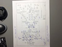
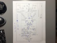
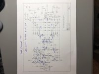
I have attached two identical schematics - one for each channel with DC voltages using a 40Vdc power supply with a DBT and one for each channel measuring AC voltages to try and trace down the issue. Which I am having trouble finding a smoking gun, so I'm here to ask for assistance. Tested with the same 0.056 input, I get 1.464 on low gain channel and 1.748 on the good channel
The only thing I have changed so far is Q10/Q12 (3502/1381) because that's where the AC difference showed up first in the schematic as I was tracing voltages (this is my first time to try this process, so I'm sure I have missed a few keys probe points, but hoped what I have provided would give some direction.
I have tested all resistors and diodes (comparing for values and comparing to the "good" channel) - everything checked out in spec. or the same as the "good" channel if anything wasn't measuring to spec. I cannot see anything gravely wrong comparing either DC or AC voltages I measured.
The "Low" channel also has 15mV of Bias, ~1mV of DC offset and plays music without distortion, just at about 5db lower volume than the other channel. Thanks for any help getting this solved.
I recently built two channels following the build guide, schematic and write-up. Used 2N5551/5401 (Q1/Q2?Q3/Q4/Q5/Q6/Q7/Q8/Q9/Q13/Q14) for small signal transistors, 2SC3503e/1381e for the VAS and bias sensing transistor (3503e) Q10/Q11/Q12, MJE340/350 for drivers (Q15/Q16) and MJL4281a/4302a for outputs.
Ironically the first channel, which I spent weeks carefully putting together has a lower gain then the second channel I put together in a weekend? I will call Channel "A" (marked as such in pictures) as the Low Gain channel and Channel "B" the Correct Gain channel. Channel 'A" has about 26 gain and Channel "B" has the correct 31 gain, according to the write-up information.
I have attached two identical schematics - one for each channel with DC voltages using a 40Vdc power supply with a DBT and one for each channel measuring AC voltages to try and trace down the issue. Which I am having trouble finding a smoking gun, so I'm here to ask for assistance. Tested with the same 0.056 input, I get 1.464 on low gain channel and 1.748 on the good channel
The only thing I have changed so far is Q10/Q12 (3502/1381) because that's where the AC difference showed up first in the schematic as I was tracing voltages (this is my first time to try this process, so I'm sure I have missed a few keys probe points, but hoped what I have provided would give some direction.
I have tested all resistors and diodes (comparing for values and comparing to the "good" channel) - everything checked out in spec. or the same as the "good" channel if anything wasn't measuring to spec. I cannot see anything gravely wrong comparing either DC or AC voltages I measured.
The "Low" channel also has 15mV of Bias, ~1mV of DC offset and plays music without distortion, just at about 5db lower volume than the other channel. Thanks for any help getting this solved.
Attachments

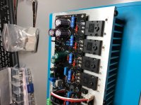
Here's some pics of the defective channel. Unsure what to test/replace next, but I hate to shotgun parts (likely starting with TO-92s), but I think I should step away for the night and hopefully have an epiphany tomorrow.
Attachments
Problem SOLVED!!!
I can’t believe I did this but I put a 0.1uF cap in C2 instead of the 470pF it should have been. In my defense they are identical size, lead spacing and color, but it’s still these bad eyes I guess. I know I looked at the markings on the sleeve at least 3 times.
Only found it because I raised a leg and put my capacitor meter on it and you can imagine my surprise when the reading comes up.
Changed C2 to the correct 470pF and my input voltage no longer drops 11mV and the output is level with the other channel now.
Now to put it all back in the case, check bias and zero the offset since I changed all the TO-92s.
Let you know what it sounds like after I e had some time with it working correctly.
Hi,
Great project, thanks for publishing.
Is Q9-C meant to connect to Q8-B (right snippet), or rather to Q8-E as in Michael Chua's original (left).
Is this your change, as noted on github...
"Added back Q9 transistor for Q8 protection"
8<
Because Q3 acts as a high impedance load, the current from Q1 is steered into the base of Q8 which is an emitter-follower configuration. This minimizes the load of Q1. Q8 is a vulnerable transistor as it drives Q10 with whatever current is necessary to maintain feedback, even when the amplifier is at the rails. To prevent the current in the collector of Q8 from exceeding safe operating limits, transistor Q9 steals base current from Q8 when the current in the VAS exceeds about 20 mA. This is one diode drop across the emitter-base of Q9 divided by resistor R19. If Q9 is not present a brief excursion into the rails can destroy Q8 as the voltage and current on it can greatly exceed tolerable limits.
/8<
I built it with boards using the Right schematic with Q9 and works great. Use the link and go to the hosted site and download the latest gerbers and they will work. Started with +\-65Vdc, went to +\-75Vdc after 4-5 months and no issues with either.
Thanks.
After reading your comments I have no doubts.
I've imported the Kicad files into Altium and made a gerber compare already. A final schematic check against the original and I'm ready to go with my own gerbers.
After reading your comments I have no doubts.
I've imported the Kicad files into Altium and made a gerber compare already. A final schematic check against the original and I'm ready to go with my own gerbers.
Actually there were several changes, but the original Q9 was a problem and ended up causing my board to smoke on multiple occasions. I also added simple stuff like hum breaker resistors, a coil on the output to prevent oscillation (potentially), a 10k resistor on the output to make sure when the amp starts it starts stably, I added other stuff like Zeners on the rails for paranoia to prevent spikes from the transformer.
I have been using this amp with my PrettyGoodAmplifier ( https://github.com/profdc9/PrettyGoodPreamplifier ) and the phono preamp ( https://github.com/profdc9/PhonoPreAmp ) day in-day out now for more than a year with no problems.
I have been using this amp with my PrettyGoodAmplifier ( https://github.com/profdc9/PrettyGoodPreamplifier ) and the phono preamp ( https://github.com/profdc9/PhonoPreAmp ) day in-day out now for more than a year with no problems.

- Home
- Amplifiers
- Solid State
- PCBs of layouts of Ampslab's C300 amplifier