I am making a layout for my active crossover as shown in the attached photo. In addition to op-amps in crossover, there are three more dual op-amps for balanced input stage biasing. With many modern op amps in a PCB, I decide to make a 4-layer-PCB layout with ground plane on layer 2, Vcc on layer 3 and Vee on layer 4.
Here I have a problem with capacitor. The capacitor in crossover is rather large in order to keep the resistance low enough. For 4.7 uF I have no choice but to use through hole capacitor (Panasonic ECW-FD)
For other capacitors, I have two choices:
1. Through hole film capacitor like Wima FKP3 or Panasonic ECW-FD. They are pretty compact and have very good characteristics. But since they are through hole part, it will create holes in ground plane. So many of them will make my PCB like a Swiss cheese.
2. NP0 (C0G) SMT capacitors: they have great characteristics, small, low inductance, don't interrupt the ground plane. But from measurement by Vicnic in "Low distortion oscillator" topics, their THD is slightly worse than some THT film caps like Wima FKP3.
There are film SMT capacitor in PPS dielectric, but they are worse than C0G ceramic and Polypropylene THT caps, so I don't want to use them.
Since I don't have much experience in analog hardware design, I would like to ask you folks which type of caps I should choose in my design, C0G SMT with an unbroken ground plane or THT film capacitor with a broken gorund plane.
Thanks,
Trung
It is a ground plane, some holes don't matter at all....it will create holes in ground plane. So many of them will make my PCB like a Swiss cheese...
Hopefully the inner layers will be flawless in the first run and making. It is really a PITA if there is something wrong: you have to start over or make bypasses. A mess....I decide to make a 4-layer-PCB layout...Since I don't have much experience in analog hardware design, I would like to ask you folks...
And why? This circuit is very simple. I do it on one layer. Two for convenience for most less design-seasoned folk.
And all those layers, all those stray capacitances. Not one, two or three dimensions, but four! Dark and swollen clouds are gathering above your head.
Generally a 2 layer PCB for a audio style op-amp board is sufficient unless you have additional high speed digital circuitry involved. A 4 layer PCB is overkill.
Check page 20 of the OPA1611 datasheet as it provides example PCB layout guidelines.
Check page 20 of the OPA1611 datasheet as it provides example PCB layout guidelines.
Thanks MarsBravo and Indiglo for your advice. So using THT film capacitor will not make the layout worse.
The circuit in post 1 is only for demonstrated purpose. Each channel in the real design will have 4 opamps for balanced input biasing, capacitance bootstrapping as well as DC remover, 3 opamps for balanced buffer output. Each of 3 outputs will also need equalisation and delay filters. Routing power tracks for more than 20 opamps from a power input socket is not too easy, that is why I am thinking to use power planes to reduce inductance in power tracks.
@MarsBravo: Do you know how to effectively route the power lines for each opamps in multiple opamps circuit without power planes? I am still learning, so every advice is appreciated.
Thanks, Trung
Generally a 2 layer PCB for a audio style op-amp board is sufficient unless you have additional high speed digital circuitry involved. A 4 layer PCB is overkill.
Check page 20 of the OPA1611 datasheet as it provides example PCB layout guidelines.
4 layer pcb from JLCPCB will be almost free. I did a 3"x4" 4 layer board last spring that cost $53 for 5 pieces
INCLUDING 2nd day air to send them to me in southern CA. I Emailed the files on a Wednesday and had the
boards in hand the following Tuesday.
To the OP: go ahead with 4 layers if it makes you happy. A couple through holes in the ground plane won't
cause any problems. When I was doing commercial boards some nodes were very sensitive to stray capacitance.
I intentionally left holes in the ground plane under those ICs.
Stay safe
G²
1. There is nothing to worry about. The difference is negligible for your purpose.But from measurement by Vicnic in "Low distortion oscillator" topics, their THD is slightly worse than some THT film caps like Wima FKP3.
2. Holes in PCB is not a problem, as for me.
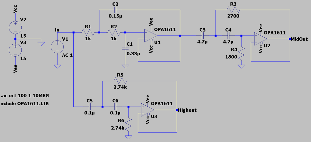
3. I don't know what crossover you do, but it seems to me that C3, C4 values are too large? It is too large for both FKP and C0G.
Last edited:
Do you know how to effectively route the power lines for each opamps in multiple opamps circuit
without power planes?
Line up the ICs all in a row (head to tail). Run two straight, parallel traces (one +V, one -V)
through the middle of all the ICs. Use the components to jumper across the lines.
Last edited:
Right! High impedance nodes are notoriously and HF feedback caps....some nodes were very sensitive to stray capacitance. I intentionally left holes in the ground plane under those ICs...
Those HF feedback caps can be bridged over the opamp or mounted on the copper side. Also an option is to have the rails parallel to mentioned row line up (on either side a rail) and hook them up in a 'distributed starpoint' with jumper wires. Decouple each opamp locally (also bridge or bottom).Line up the ICs all in a row (head to tail). Run two straight, parallel traces (one +V, one -V) through the middle of all the ICs. Use the components to jumper across the lines.
- Home
- Design & Build
- Construction Tips
- PCB design trade-off