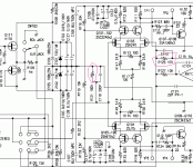
Hello all,
I was looking at this schematic and was wondering why the negative feedback resistor (R125) is 47K and not 100K? Could it be a mistake on the schematic or am I missing something.
The input resistor (R121) to ground is 100K.
I don't own this amp but I am trying to understand the design.
Thanks.
I was looking at this schematic and was wondering why the negative feedback resistor (R125) is 47K and not 100K? Could it be a mistake on the schematic or am I missing something.
The input resistor (R121) to ground is 100K.
I don't own this amp but I am trying to understand the design.
Thanks.
Attachments
In well-balanced BJT inputs it is good habit to make the DC resistance equal on both sides to cancel base current errors.
This is a JFET input. No base current. (Gate current is negligible.) Moreover it is complementary giving some cancellation of opposing (negligible) gate currents. Moreover there is a DC Servo to force the output to zero despite input errors.
This is a JFET input. No base current. (Gate current is negligible.) Moreover it is complementary giving some cancellation of opposing (negligible) gate currents. Moreover there is a DC Servo to force the output to zero despite input errors.
Attachments
Last edited:
Input resistor and negative feedback resistor valuecan be different, it depend on the circuit design. One of the negative feedback function is for the gain control, feedback resistor (R125) & resistor (R106) do the gain control job.