Good evening DIYaudio
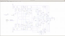
I am a university student studying EE (years ago I studied ME). In the past year I have spent countless hours trying to complete a schematic for an amplifier that would work well for SE input and could power bookshelf, headphones, or possibly use as a fixed output preamp. Basically a versatile low power amplifier that could be biased into class A.
I give credit to others for the design, as there is quite a bit of others (some quite well known around here) fairly well published work principally making up the design. I do not take much credit for anything other than adapting existing topology to meet what I was hoping to achieve. I admit the parts count is a little bit high, but the simulation looks promising.
I am a complete novice and although I have a basic understanding of the functioning mechanisms of the amplifier I would greatly appreciate others with much more experience that have the time to look it over. I may have done things that won't work or have left out important parts. I know I am missing a zobel network on the output and I would like to add diode protection for the output FETs.
If it does seem to be reasonable to build, I have not much of a clue where to start with PCB design, so recommendation of any reference materials to read or design guidelines is greatly appreciated.
Attachments
Look at Bob Cordell's DH-220C design, (the presentation is a utube video from a burning amp meeting) it is basically the same as yours except it uses lateral fets (as used in the hafler DH-220) and it is tested and proven to work.
The bias generator needs to be changed so that it senses the HS temp and can compensate for bias current changes when the vert fets o/p's warm up.
It is a lot to be able to explain all the caveat's in designing a pcb in one thread.
Once you look at the DH-220C design, you will see where your design needs improvements
The drivers can charge up the output device gates fast (there's no current limit), butcan only discharge via the 6k04 resistor. I think that's going to be switching distortion at HF, or even supercharge the bias and burn out the output devices at high amplitude HF.
I think R27 needs a parallel capacitor to sort this out.
Relatedly Q9 and Q10 have vulnerable base-emitter junctions that could see reverse bias at times, backwards diodes across them might be wise.
You have one feedback network trying to balance out both differential pairs, it can't do both.
Separate DC servos might be a way round that, but easier is losing one diff pair and load the VAS with a current source/sink. That will also make compensation much simpler.
There's no gate protection for the output MOSFETs, in fact various protection precautions
could be added, like rail-gnd diodes, output current limiting, making it less delicate.
So worked at it quite a bit more and a few updates thanks to the advice provided.
Thanks I've found the thread, and it is very helpful. Maybe I should just get one of those pcbs lol?? Most of this design can be accredited to Borbely and Cordell. Just putting the blocks together.
I tried to use a transistor as a diode, but because of the high Vth values .7V doesn't account for very much. I will have to make changes to get the bias spreader to be more equal across the transistors.
Thanks for the suggestion. I simply added the 100p and 100r used in the above referenced schematic and it did settle things down quite a bit providing much better simulation numbers. I was suprised at the .007 @ 20k and .0018 @ 1k, 4 ohm load, 8VRMS out. There still is some ringing, but only on the order of a few dB. Not sure if this is problematic. I originally had planned on using dual CCS, then decided it was too much trouble, but I have changed back. It allows for a compromise between transconductance matching and a manageable level of offset. I will get on to the next steps of current limiting but because the maximum voltage across the drivers is only 11.3V I can't use a set of diodes in series (because of the bias spread ~8.5V).
Hopefully this project of mine is viable enough to make it to a protoboard this summer. Appreciate the help.
(change the .lib.txt to .lib wouldn't let me upload)
Look at Bob Cordell's DH-220C design, (the presentation is a utube video from a burning amp meeting) it is basically the same as yours except it uses lateral fets (as used in the hafler DH-220) and it is tested and proven to work.
The bias generator needs to be changed so that it senses the HS temp and can compensate for bias current changes when the vert fets o/p's warm up.
It is a lot to be able to explain all the caveat's in designing a pcb in one thread.
Once you look at the DH-220C design, you will see where your design needs improvements
Thanks I've found the thread, and it is very helpful. Maybe I should just get one of those pcbs lol?? Most of this design can be accredited to Borbely and Cordell. Just putting the blocks together.
I tried to use a transistor as a diode, but because of the high Vth values .7V doesn't account for very much. I will have to make changes to get the bias spreader to be more equal across the transistors.
The drivers can charge up the output device gates fast (there's no current limit), butcan only discharge via the 6k04 resistor. I think that's going to be switching distortion at HF, or even supercharge the bias and burn out the output devices at high amplitude HF.
I think R27 needs a parallel capacitor to sort this out.
Relatedly Q9 and Q10 have vulnerable base-emitter junctions that could see reverse bias at times, backwards diodes across them might be wise.
You have one feedback network trying to balance out both differential pairs, it can't do both.
Separate DC servos might be a way round that, but easier is losing one diff pair and load the VAS with a current source/sink. That will also make compensation much simpler.
There's no gate protection for the output MOSFETs, in fact various protection precautions
could be added, like rail-gnd diodes, output current limiting, making it less delicate.
Thanks for the suggestion. I simply added the 100p and 100r used in the above referenced schematic and it did settle things down quite a bit providing much better simulation numbers. I was suprised at the .007 @ 20k and .0018 @ 1k, 4 ohm load, 8VRMS out. There still is some ringing, but only on the order of a few dB. Not sure if this is problematic. I originally had planned on using dual CCS, then decided it was too much trouble, but I have changed back. It allows for a compromise between transconductance matching and a manageable level of offset. I will get on to the next steps of current limiting but because the maximum voltage across the drivers is only 11.3V I can't use a set of diodes in series (because of the bias spread ~8.5V).
Hopefully this project of mine is viable enough to make it to a protoboard this summer. Appreciate the help.
(change the .lib.txt to .lib wouldn't let me upload)
Attachments

Last edited:
I made some errors in the previous sch posted. Staying up way to late staring at a simulation trace until the early morning hours doesn't always give the best results. I think I've found some more accurate models for the mosfets and a better suited pair used in a popular low power amp. Seems to have fairly similar results with minor variation in components and values, AC analysis is fairly decent so I will order the parts and put on a protoboard with fingers crossed.
I still need to change bias spreader to include thermal comp., choose a more appropriate D7, D8, and hope to add some form of current limiting but for now I think I have made enough headway to purchase a few components.
I still need to change bias spreader to include thermal comp., choose a more appropriate D7, D8, and hope to add some form of current limiting but for now I think I have made enough headway to purchase a few components.
Attachments
Thank you for your guidance Mr. Tillotson
hope its not to late
thats a unique CMOS VBEX 😀
hope its not to late
thats a unique CMOS VBEX 😀
Last edited:
- Home
- Amplifiers
- Solid State
- Feedback request.. 32W amplifier 14x32 student design