As some of you may know I am putting together a website about switch mode power supplies and Class D amplifiers.
I've 'kind of' finished off the theory stuff about the switch mode power supply and moved on to the Class D amplifier part.
Whilst going through the motions I hit another 'thing'.
Cross over distortion due to dead time. I'd heard about it but never really thought about it..... then it 'appeared'. Now I might have to think about it.
Anyway, if you fancy a look then,
http://www.genomerics.org/outfilt.html
Home page is at
http://www.genomerics.org/index.html
Sorry it was just one of those GOSH moments
Cheers
DNA

Hi DNA,
I find the dead time induced distortion to be one, if not the most important root of distortion in class D's.
I also find it interesting in that no manufactures have jumped on the "class A~D" version of this. I'm sure they will come.
Its not nearly as bad as real class A vs class B, it just means you need to run the ripple current inductor very high, such that the peaks of the current are higher than the maximum expected output current. Yes the effeciency will be lower if all else stays the same, but it will still be better than any class AB on its best day! (Except maybe at idle.)
I'm planning to get around to doing some experiements with a UcD400 and smaller filter inductance, larger output caps....
Nice pictures on your site!
Mike
flo said:Hi DNA,
Great website! Very informative and fun to read.
Can't wait for the next update
Florian
I had to take my head out of my bum to read this. Now I have to try and put it back in again.


Thanks, may all your breakfasts be seriously tasty.
Cheers
DNA
Hello DNA,
It's been discussed on this forum before, but you are seeing the curious effect on deadtime of the peak-to-peak current of the output inductor current of a class-d amplifier. As long as the output inductor current ripple is larger than the load current at the moment of switching, its current is in the right direction to force the output stage node voltage to begin slewing to the other rail immediately when both MOSFETs turn off at the beginning of deadtime (this is natural commutation - also known as soft switching). For larger load currents, slewing doesn't commence until the end of deadtime when the other MOSFET forces the voltage to change. Thus, unlike a linear class-b amplifier (where deadtime is at zero output) there are two deadtime zones at non zero load current (symmetrically spaced about zero). Nice web site, by the way.
Regards -- analogspiceman
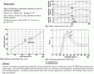
Here's a reference to a very good short technical letter on the subject of class-d deadtime distortion:
Effect of dead time on harmonic distortion in class-D audio power amplifiers
Mosely, I.D. Mellor, P.H. Bingham, C.M.
Dept. of Electr. & Electron. Eng., Machines & Drives Group, Sheffield
This paper appears in: Electronics Letters
Publication Date: 10 Jun 1999
Volume: 35 , Issue: 12
On page(s): 950 - 952
ISSN: 0013-5194
CODEN: ELLEAK
INSPEC Accession Number:6290250
Digital Object Identifier: 10.1049/el:19990705
Posted online: 2002-08-06 22:36:47.0
Abstract
A model is described for predicting the harmonic levels introduced by the use of dead time in class-D, PWM-driven audio power output stages. The model demonstrates that the harmonic levels are a function of load impedance, modulation depth, dead time and switching frequency. In addition, measurements show that, for audio applications, dead time is the dominant cause of power stage non-linearity.
Citing Documents
An integrated 200-W class-D audio amplifier, Berkhout, M.
Solid-State Circuits, IEEE Journal of
On page(s): 1198- 1206, Volume: 38, Issue: 7, July 2003
A 20-W stereo class-D audio output power stage in 0.6-/spl mu/m BCDMOS technology, Morrow, P.; Gaalaas, E.; McCarthy, O.
Solid-State Circuits, IEEE Journal of
On page(s): 1948- 1958, Volume: 39, Issue: 11, Nov. 2004
A current-mode power sigma-delta modulator for audio applications, Dallago, E.; De Leo, G.; Sassone, G.
Industrial Electronics, IEEE Transactions on
On page(s): 236- 242, Volume: 52, Issue: 1, Feb. 2005
It's been discussed on this forum before, but you are seeing the curious effect on deadtime of the peak-to-peak current of the output inductor current of a class-d amplifier. As long as the output inductor current ripple is larger than the load current at the moment of switching, its current is in the right direction to force the output stage node voltage to begin slewing to the other rail immediately when both MOSFETs turn off at the beginning of deadtime (this is natural commutation - also known as soft switching). For larger load currents, slewing doesn't commence until the end of deadtime when the other MOSFET forces the voltage to change. Thus, unlike a linear class-b amplifier (where deadtime is at zero output) there are two deadtime zones at non zero load current (symmetrically spaced about zero). Nice web site, by the way.
Regards -- analogspiceman
Here's a reference to a very good short technical letter on the subject of class-d deadtime distortion:
Effect of dead time on harmonic distortion in class-D audio power amplifiers
Mosely, I.D. Mellor, P.H. Bingham, C.M.
Dept. of Electr. & Electron. Eng., Machines & Drives Group, Sheffield
This paper appears in: Electronics Letters
Publication Date: 10 Jun 1999
Volume: 35 , Issue: 12
On page(s): 950 - 952
ISSN: 0013-5194
CODEN: ELLEAK
INSPEC Accession Number:6290250
Digital Object Identifier: 10.1049/el:19990705
Posted online: 2002-08-06 22:36:47.0
Abstract
A model is described for predicting the harmonic levels introduced by the use of dead time in class-D, PWM-driven audio power output stages. The model demonstrates that the harmonic levels are a function of load impedance, modulation depth, dead time and switching frequency. In addition, measurements show that, for audio applications, dead time is the dominant cause of power stage non-linearity.
Citing Documents
An integrated 200-W class-D audio amplifier, Berkhout, M.
Solid-State Circuits, IEEE Journal of
On page(s): 1198- 1206, Volume: 38, Issue: 7, July 2003
A 20-W stereo class-D audio output power stage in 0.6-/spl mu/m BCDMOS technology, Morrow, P.; Gaalaas, E.; McCarthy, O.
Solid-State Circuits, IEEE Journal of
On page(s): 1948- 1958, Volume: 39, Issue: 11, Nov. 2004
A current-mode power sigma-delta modulator for audio applications, Dallago, E.; De Leo, G.; Sassone, G.
Industrial Electronics, IEEE Transactions on
On page(s): 236- 242, Volume: 52, Issue: 1, Feb. 2005
Attachments
Portlandmike said:Hi DNA,
I find the dead time induced distortion to be one, if not the most important root of distortion in class D's.
I also find it interesting in that no manufactures have jumped on the "class A~D" version of this. I'm sure they will come.
Its not nearly as bad as real class A vs class B, it just means you need to run the ripple current inductor very high, such that the peaks of the current are higher than the maximum expected output current.
Nice pictures on your site!
Mike
Pictures are courtesy of LTspice and Xnview. LTspice lets me copy a 'bitmap' to the clipboard and then I can fiddle about with it in Xnview to crop it and turn it into a .gif file.
There is something going on in there. 200nS/2.5uS is 0.08. Also 50 + 50 is 100 and the 'blip' happens at 8V so, well I don't know. It's going to take some staring at but I'm sure someone else has explained it elsewhere.
Like I said it was a GOSH thing because, although I'd heard about it, I'd never seen it before. I mentioned it because it's a cute thing to see.
DNA
analogspiceman said:Hello DNA,
It's been discussed on this forum before, but you are seeing the curious effect on deadtime of the peak-to-peak current of the output inductor current of a class-d amplifier. As long as the output inductor current ripple is larger than the load current at the moment of switching, its current is in the right direction to force the output stage node voltage to begin slewing to the other rail immediately when both MOSFETs turn off at the beginning of deadtime (this is natural commutation - also known as soft switching). For larger load currents, slewing doesn't commence until the end of deadtime when the other MOSFET forces the voltage to change. Thus, unlike a linear class-b amplifier (where deadtime is at zero output) there are two deadtime zones at non zero load current (symmetrically spaced about zero). Nice web site, by the way.
Regards -- analogspiceman
Thanks! That makes so much sense that I am feeling slightly stupid. I could have spent ages scratching my head over it...
DNA
Genomerics said:Thank you analogspiceman, I have just quoted you on the website. I'll try to explain things better tomorrow.
If you want me to scrub that one then say so.
If you think it promotes understanding, then quote away, by all means...

But perhaps, for the sake of better accuracy and clarity, I could ask you to make a slight correction to the text (replace "its current is in the right direction" so the text will read as follows):
It's been discussed on this forum before, but you are seeing the curious effect on deadtime of the peak-to-peak current of the output inductor current of a class-d amplifier. As long as the output inductor current ripple is larger than the load current at the moment of switching, the sum of the two currents is in the right direction to force the output stage node voltage to begin slewing to the other rail immediately when both MOSFETs turn off at the beginning of deadtime (this is natural commutation - also known as soft switching). For larger load currents, slewing doesn't commence until the end of deadtime when the other MOSFET forces the voltage to change. Thus, unlike a linear class-b amplifier (where deadtime is at zero output) there are two deadtime zones at non zero load current (symmetrically spaced about zero).
Regards -- analogspiceman
Hello AnalogSpiceman,
While I'm aware of the existence of the paper on dead time vs distortion, I have yet to get around to read it, but your attached pdf page leaves me cold, for they talk about very high distortion levels. Latest breed of class-D amps have THD lower than 0.01%.
One collorary of the summary you presented could be that there would be no "crossover distortion" if there were no dead time?
On the other hand, my simple and intuitive explanation of no cross over distortion in class-D amp is in the absence of discontinuity around zero crossing of the input (modulating) signal, just like class-A has no crossover distortion due to absence of any discontinuity around zero input.
I'm also AES and IEEE member.
Originally posted by koolkid731
While I'm aware of the existence of the paper on dead time vs distortion, I have yet to get around to read it, but your attached pdf page leaves me cold, for they talk about very high distortion levels. Latest breed of class-D amps have THD lower than 0.01%.
One corollary of the summary you presented could be that there would be no "crossover distortion" if there were no dead time?
The graphs apply to a design with a deadtime that seems to be set purposefully high in order to better illustrate the authors' point. Deadtime is 10 percent of the switching period (Td = 1us at fs = 100kHz). Bear in mind that the reported distortion is for the modulator/power stage unmoderated by any feedback. A practical class-d design might have 25dB or so of feedback available to reduce the already small distortion arising from its typically less than 1 percent deadtime. (And that should just about spin the THD numbers down to your comfort zone.)

By the way, I think Bruno already wrote an entire book about that corollary you posted (it's arguably the keystone of the UcD's simple, yet elegantly high performing design).
Regards -- analogspiceman
Hello again
I've just uploaded the first part of the explanation as to what is going on. It looks like there are two things that need to be accounted for.
The first is a DC offset (just done that) and the second is the point at which this occurs (Too be Done).
Cheers
DNA
http://www.genomerics.org/outfilt.html
I've just uploaded the first part of the explanation as to what is going on. It looks like there are two things that need to be accounted for.
The first is a DC offset (just done that) and the second is the point at which this occurs (Too be Done).
Cheers
DNA
http://www.genomerics.org/outfilt.html
Well, I've finished explaining/describing what is going on.
http://www.genomerics.org/outfilt.html
There are two parts to it. One is a DC offset on the output above a certain output level. The second is the 'plateau' that appears in the output waveform.
It might not be 100% but hopefully it's useful to see.
Cheers
DNA
http://www.genomerics.org/outfilt.html
There are two parts to it. One is a DC offset on the output above a certain output level. The second is the 'plateau' that appears in the output waveform.
It might not be 100% but hopefully it's useful to see.
Cheers
DNA
Genomerics said:Well, I've finished explaining/describing what is going on.
http://www.genomerics.org/outfilt.html
There are two parts to it. One is a DC offset on the output above a certain output level. The second is the 'plateau' that appears in the output waveform.
It might not be 100% but hopefully it's useful to see.
Cheers
DNA
DNA,
Excellent work. You might point out, or show too, that dead time distortion causes "error pulses" when the output current exeeds the inductor ripple current. Thus, it increases with frequency, since you get more error pulses because you transistion thru the ripple current sweat spot more often.
If so inclined, an FFT of the results would be good to see. You will find that dead time induced distortion is NOT nice at all, in that its odd order, and is not limited to low orders.
It seems to me a Class D design with very high ripple current would be ideal in that the main source of distortion would be minimized. It still exists, in that now its the body diode voltage rather than the whole rail, but that's not much.
By that point, I think the model falls apart since allowing some cross conduction can actually eleminate the body diode from ever comming on.
There is also a paper that shows that adding some capacitance to the switch node can minimize this distortion. This is shown to help, but has obvious disadvantages in effeciency.
Regards
Mike
quote from www.genomerics.org:
Ultimately the effects arise because the filter is not being driven by a true voltage source and there are times when it is inductor current rather that the PWM signal that is determining the input voltage to the filter.
I do not think it can be explained any clearer. If dead time per se would be a problem, then class BD (three state) modulation would not work.
Regarding high ripple current in output stage, it might even boost efficiency. By using very large FETs you compensate for conduction losses, while at the same time large inductor current helps to achieve ZVS over full operating range. Adding external capacitors across switches is a common practice when those are operating at ZVS conditions.
Best regards,
Jaka Racman
For Portland Mike
I think I've shown that when output current exceeds the ripple current then the inductor current forces deadtime to favour the opposite rail and that is where the 'offset' comes from. Perhaps I haven't stated it in those terms..... OK, maybe I should include a better summary of what I think I have said.
I've set the model for dpowmodb.asc back to the original 1KHz drive with 200nS delay in the gate that determines deadtime.
Like I say, every so often, if you want to have a play with the models I am using then clicking on the Linear Technology logo should let you download the .asc file. Mind you, I've spotted something in there that might mess things up if you push things too far.
I wouldn't want to start talking/thinking about even or odd harmonic distortion and the relative niceties of them. Since the effect is symmetrical about zero then it has to be odd order(?) and, while it's there there's not much to be done other than find a way of minimising it.
Fair enough, it would seem that operating with 'high' ripple currents would 'solve' the problem but then that starts to mess with the performance of the filter, maybe (and other stuff).
On the other hand operating with 'higher' ripple currents moves the problem to higher output levels and now we have the opportunity to use an engineering problem for marketing purposes.
'Dead time and output filter ripple optimised for powerful performance without compromising low level detail'
Until I saw it happening I was thinking about something to do with the forward voltage of the DS diodes being the source of the problem. Now I've seen it I know I was wrong.
I suppose, once it's gone then we're left with matching of components...... Even if you turn the mosfets on you can't avoid the diodes carrying some current but, if the mosfets are not matched then..... And then if you can't guarantee delay times and switching times... Then what?
I'd have to have a poke about with adding capacitance to the switched node but my 'gut' feeling is it's just going to introduce more problems and make the original one appear elsewhere or not go away anyway.
Cheers
DNA
Jaka Racman said:
I do not think it can be explained any clearer. If dead time per se would be a problem, then class BD (three state) modulation would not work.
Regarding high ripple current in output stage, it might even boost efficiency. By using very large FETs you compensate for conduction losses, while at the same time large inductor current helps to achieve ZVS over full operating range. Adding external capacitors across switches is a common practice when those are operating at ZVS conditions.
Best regards,
Jaka Racman
Jaka,
The only examples of three states I've seen are very old, and had pretty poor distortion. Are there any modern examples? The ones I saw also work in such a way that they always have ripple current higher than the output current. If not, they'd have plenty of distortion with a similar inductor current delay related distortion.
That is, the swich node would not even commutate to the other state until the inductor current crossed zero?
Running at high current is NOT ZVS. There are still significant switching losses only they happen when the swich is shutting off, and for example the switch current is less than the inductor current (so the swich node begins to slew to the other rail, and when it has volts and amps on the turning off swich. I never seen the ZVS term applied to a "buck" type regulator, and I think this is the reason. Its not ZVS, correct me if I'm wrong.
I agree effeciency is not the biggest reason not to do it, its cost. physically larger inductors, more or better local bypass caps, more required output cap, but still, compared to the penalty for linear class A (like heat sinks and the power supply, its quite trivial.)
One thing that does perhaps minimize the benifit is that in examples such as the UcD400, which I've looked at, the dead time error seems to be minimized by well controlled turn on and turn off of the fets with minimal, but not non-existant cross conduction. But I still wanna try it
Best Regards,
Mike
Genomerics said:For Portland Mike
I think I've shown that when output current exceeds the ripple current then the inductor current forces deadtime to favour the opposite rail and that is where the 'offset' comes from. Perhaps I haven't stated it in those terms..... OK, maybe I should include a better summary of what I think I have said.
I've set the model for dpowmodb.asc back to the original 1KHz drive with 200nS delay in the gate that determines deadtime.
Like I say, every so often, if you want to have a play with the models I am using then clicking on the Linear Technology logo should let you download the .asc file. Mind you, I've spotted something in there that might mess things up if you push things too far.
I wouldn't want to start talking/thinking about even or odd harmonic distortion and the relative niceties of them. Since the effect is symmetrical about zero then it has to be odd order(?) and, while it's there there's not much to be done other than find a way of minimising it.
Fair enough, it would seem that operating with 'high' ripple currents would 'solve' the problem but then that starts to mess with the performance of the filter, maybe (and other stuff).
On the other hand operating with 'higher' ripple currents moves the problem to higher output levels and now we have the opportunity to use an engineering problem for marketing purposes.
'Dead time and output filter ripple optimised for powerful performance without compromising low level detail'
Until I saw it happening I was thinking about something to do with the forward voltage of the DS diodes being the source of the problem. Now I've seen it I know I was wrong.
I suppose, once it's gone then we're left with matching of components...... Even if you turn the mosfets on you can't avoid the diodes carrying some current but, if the mosfets are not matched then..... And then if you can't guarantee delay times and switching times... Then what?
I'd have to have a poke about with adding capacitance to the switched node but my 'gut' feeling is it's just going to introduce more problems and make the original one appear elsewhere or not go away anyway.
Cheers
DNA
DNA,
Please don't let me make more work for you, you've done an exellent tutorial.
If your interested though, body diodes need not conduct in the ideal world. That is, the turning on swich need not wait for the turning off swich to be all the way off.
Matching? I suspect its not that important. Could be wrong though.
You'll also find that how fast the nodes slew is not an issue, besides effeciency and EMI, but not for distortion. It doesn' t even need to be the same both ways If I recall.
In the real world I think you can run at high ripple currents and move the dead time distortion down lots. It will show up a diode body voltage pulse, but this is small compared to the rail voltage amplitude spikes.
The next biggest distortions I suspect are the modulator operating in a very noisy enviornment, not easy to simulate without lots of homework.
Bruno P. would say that delay doesn't matter if you design it in
A+ work.
Mike
Hi Mike,
I could not find a better link regarding ZVS, the article I had in mind is not available any more but here it is:
ZVS Buck converter
Best regards,
Jaka Racman
P.S. TAS5015 is TI digital BD class modulator. Tact Millenium and prototypes of John W use it with impressive results.
I could not find a better link regarding ZVS, the article I had in mind is not available any more but here it is:
ZVS Buck converter
Best regards,
Jaka Racman
P.S. TAS5015 is TI digital BD class modulator. Tact Millenium and prototypes of John W use it with impressive results.
- Status
- This old topic is closed. If you want to reopen this topic, contact a moderator using the "Report Post" button.
- Home
- Amplifiers
- Class D
- Dead Time and Crossover Distortion