D
Deleted member 148505
Interesting!
Tried antiparallel diodes on gate resistors. No change.
What is your switching freq?
All with no snubbers?
So you also use gate buffers in this design?
Post a picture?
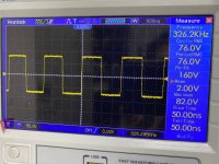
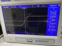
Switching freq around 320kHz. Snubber 10R + 100pf.
bypass / decoupling caps right at the mosfet pins.
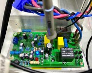
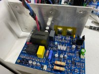
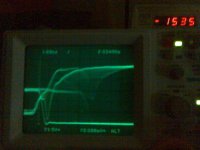
Green PCB output mosfet is IPP320N20N3, no gate buffers, only 10R + 1n4148 + 4.7R for gate turn off.
Scope traces are from the green PCB.
I used ZXGD on the blue PCB prototype, but it uses IRFB4227. Also I don't have scope traces of the blue PCB because I already sent it on the other side of the globe for evaluation.
Attachments
Waooo nice result.
The first yellow cap from left is that decoupling from rail to rail?
I'm even using SMD ....
My results must then be down to layout and not enough decoupling :|
The first yellow cap from left is that decoupling from rail to rail?
I'm even using SMD ....
My results must then be down to layout and not enough decoupling :|
D
Deleted member 148505
Yes yellow is for rail to rail decoupling.
Might also be a problem with your scope probe, did you try to test other class-d amps?
Might also be a problem with your scope probe, did you try to test other class-d amps?
Of course the dent in d-s capacitance vs. Vd-s in newer faster MOSFET will awaken any hidden demons (resonances) in the layout. But these chips switch fast and abrupt. 
Then there is the chasing ghosts phenomena, a 10:1 or 100:1 probe getting substantial ground loop ringing, or a 1:1 causing ringing itself due to good 50~100pF of input capacitance.
And there are plenty of slower chips for slower layouts.
Then there is the chasing ghosts phenomena, a 10:1 or 100:1 probe getting substantial ground loop ringing, or a 1:1 causing ringing itself due to good 50~100pF of input capacitance.
And there are plenty of slower chips for slower layouts.
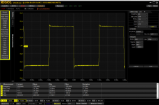
Lets remember some switching speed. 2 Layer PCB. SMD on both layers. TO-220 IRFB4227. IR drivers. Zetex buffers. Gate OFF: 1500W 33% duty shown. Gate ON: 4500W 33% duty shown. Reaching 150V/7ns transients.
(But be aware that even though this was for a product that has been producing money for 10 years, the company refused to continue sharing the money.)
(But be aware that even though this was for a product that has been producing money for 10 years, the company refused to continue sharing the money.)
Attachments

Last edited:
Of course the dent in d-s capacitance vs. Vd-s in newer faster MOSFET will awaken any hidden demons (resonances) in the layout. But these chips switch fast and abrupt.
The Ultra Junction[superjunction] Mosfet design team at IXYS confirmed, it has nothing to do with the PCB layout, no matter how tight you make it, problem is inherent to Gate construction, the noise is much higher than planar mosfets.
Last edited:
Interesting thread! How do we identify if a MOSFET is planar? Manufacturers have all kinds of superduper names for their devices.
Thought I had found the ultimate MosFet for class D
Have been experimenting IPP320N20N3 instead of my usual IRFB5620.
I really though one of my boards was fried as I en the first test got massive ringing.
I mounted another board up with IRFB5620. Only limited ringing (before mounting of snubbers).
Then changed to IPP320N20N3 ...... see pictures!!!
Boards based on IRS2092 with ZXGD3003E6 buffers and 4R7 gate resistors.
Pre + post filter fb.
Data sheet would suggest this is a real good MosFet, fast, lower Rds(on), higher current capability, low Ciss ... all in all better than IRFB5620 !!
Anyone having experience with these Fets?
What am I missing here?
So same circuitboard (layout) same resistor values, only two different MOSFETs.
The parasitic inductances are the same. Ringing is caused by excitation of inductance, the ringing frequency is a combination of capacitances with the inductance. Ringing amplitude (or overshoot) is due to L*di/dt. So if the di/dt is greater, the peak is greater. If the ringing lasts longer, the capacitance is larger. The difference is therefore due to a device that pulls the edges up and down faster, which must mean it has higher gm, and also has more parasitic capacitance.
The par-capacitance may be similar at high voltages, but at the lower voltages where it gets extremely non linear and goes sky high is perhaps where the major differences are. And all MOSFETs are always shown with different graphs, some log-log, some log-lin, all at different zooms, etc.
The interesting part is taming it. According to kASD it is inherent in the MOSFET, at least in some MOSFETs, and not controllable thru Rg very interesting.
EVA also has a very important point in that probing these fast edges is almost impossible to do with 100% certanty.
The Ultra Junction[superjunction] Mosfet design team at IXYS confirmed, it has nothing to do with the PCB layout, no matter how tight you make it, problem is inherent to Gate construction, the noise is much higher than planar mosfets.
I agree with this, its a pure periodic table material issue.
I do have a question around the ZXGD3003E6 whats the best way to construct a circuit to changing turn on/off timing without the need for RCD.
Thanks.
I agree with this, its a pure periodic table material issue.
Hmm. Same manufacturers have different type switching MOSFETs. Surely they use the same silicon? Or do they have different purities in different batches?
I thought semiconductor devices are mostly made different by varying the width and length of the channel? Then you must add the connections between the die and package pads/pins, which will have various inductive/capacitive/resistive properties.
I think it's more a geometry issue than materials issue.
Then again we have the 'rusty bolt effect' where nonlinearities appear because of junctions between various conducting materials, creating intermodulation distortion... Are we at that level looking into the physics of the chip? I think the parasitics that are a product of the geometry totally dominates.
The Ultra Junction[superjunction] Mosfet design team at IXYS confirmed, it has nothing to do with the PCB layout, no matter how tight you make it, problem is inherent to Gate construction, the noise is much higher than planar mosfets.
I experienced the problem of "gate kickback oscillation" a long time ago with FCP36N60N in a PFC, even though it was soft switched, turning off into a capacitor.
It was fixed by tweaking drive impedance as seen from the gate at ~80Mhz where the oscillation was. It needed a particular resistance to inductance ratio.
Of course layout means impedances, not tightness. This is a serious misconception.
Blah blah expensive dinner team blah blah.
Keep in mind that some times the same FET model but from another manufacturer can make a noticeable difference, my own experience although not with a class-D amp but with an SMPS product is that while working in the lab developing and doing EMC measurements (the company I worked for back then had their own accredited EMC lab) the SMPS product eventually looked fine and ready for production.
A while later we received a sample from the subcontractor and I would take it to the EMC lab and measure it, it was really noisy and didn't by far conform with the EMC standards, up to the lab and disassemble the SMPS and I found out the main switching FET was the same model, in this case IRF840, but from another manufacturer, changed the device to one from IR, back to the EMC lab and it went through fine again, so we had to tell the subcontractor to not use any other manufacturer than IR.
A while later we received a sample from the subcontractor and I would take it to the EMC lab and measure it, it was really noisy and didn't by far conform with the EMC standards, up to the lab and disassemble the SMPS and I found out the main switching FET was the same model, in this case IRF840, but from another manufacturer, changed the device to one from IR, back to the EMC lab and it went through fine again, so we had to tell the subcontractor to not use any other manufacturer than IR.
And the other thing that proved to be effective was to add a few dozen pf SMD as close to terminals as possible (allowing lower drive resistance that way).
(Field Application Team)
(Field Application Team)
Page 2 Onwards, problem accepted already by manufacturers but some idiots still beating the same old bush...
https://www.onsemi.com/pub/Collateral/AND9893-D.PDF
https://www.onsemi.com/pub/Collateral/AND9893-D.PDF
Having faster switch on and off times will cause more ringing.
The back emf of the inductor is proportional to switching on/off rise/fall times.
Higher value gate resistors or a snubber on the gate will help.
The back emf of the inductor is proportional to switching on/off rise/fall times.
Higher value gate resistors or a snubber on the gate will help.
- Home
- Amplifiers
- Class D
- Massive ringing with IPP320N20N3