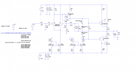
Hello, I made a simple amplifier, for learning purpose, with resistive load.
Here the schematic:

Amplifier — ImgBB
This AB amp even without load is unstable, I can't get a stable 0 voltage at the output. Sometimes is few millivolt and is ok, sometimes is at the same level of the positive or negative supply rail (24V), sometimes start from +/- 24V and than slowly goes to 0V and keep this voltage for time and then again unstable.
This happen without input signal, only with DC polarization.
With connected load is totally unstable, never I get 0V at the output, but only negative or positive supply voltage.
When is stable it can amplify an input signal (without load) with good sine waveform, no HF oscillations, but still remains the DC instability, so the amplification doesn't last long.
With Spice is everything good, I have 40mV at the output. The PCB is with SMD components only output transistors are TH with heatsink.
Can you help me to understand why?
I know there are errors but DC point should be stable with this schematic.
Here the schematic:
Amplifier — ImgBB
This AB amp even without load is unstable, I can't get a stable 0 voltage at the output. Sometimes is few millivolt and is ok, sometimes is at the same level of the positive or negative supply rail (24V), sometimes start from +/- 24V and than slowly goes to 0V and keep this voltage for time and then again unstable.
This happen without input signal, only with DC polarization.
With connected load is totally unstable, never I get 0V at the output, but only negative or positive supply voltage.
When is stable it can amplify an input signal (without load) with good sine waveform, no HF oscillations, but still remains the DC instability, so the amplification doesn't last long.
With Spice is everything good, I have 40mV at the output. The PCB is with SMD components only output transistors are TH with heatsink.
Can you help me to understand why?
I know there are errors but DC point should be stable with this schematic.
Doesn't seem like it's anything fundamental, but stability seems dubious to me.
Please add a Zobel network (~47n + 6R8 or so) at the output at the very least, an output inductor and resistor (~1.5 µH || 4R7, typ) would be good as well.
The input stage is too hot at 3.4 mA tail current IMHO, try reducing that to ~1 mA and adding ~150-220 ohm emitter degeneration resistors, increasing R1 as needed.
Neither DC resistance nor AC impedance at both inputs are balanced. Try R10 = 23.8k, R21 = R9 + C2, with your SINE adjusted to short of 1 V.
C2 is a bit on the small side, try more like 47-100µ.
So I understand you have built this and the real thing tends to latch up but simulation is fine? Then I would suspect that you have either misconnected something or that either of the inputs is lacking a DC path to either the output or ground. Have you verified that all your current sources are operating properly and checked output stage bias?
I don't see anything that would make this amplifier latch to the rails, although I see some things I don't like.
Basically, you've made a wiring error, you have bad components, or you have a bad solder joint or short. From the erratic behavior, I'm guessing a bad solder joint, and at least one other problem.
Basically, you've made a wiring error, you have bad components, or you have a bad solder joint or short. From the erratic behavior, I'm guessing a bad solder joint, and at least one other problem.
I don't add Zobel because the load is pure resistive, not a speaker.
Ok for less current and emitter resistor, I'll try.
I know tail pair is not well balanced, R21 and R10 are in the real a 25K trimmer, set to get R10=22.7K and R21=3.3K not a well solution but it's so now.
R13+R17 are 100 ohm trimmer, to adjust bias current, also here not the best implementation.
I soldered two different boards with new components, everyone tested, so I exclude bad components or bad wiring or connections for sure. I checked so many times.
A bad solder joint? Maybe, is difficult to see.
Current mirrors work I suppose, because sometimes the amp works, is stable, I can send a signal and see the output, sometimes it latches to the supply rails.
With the load it latches every time to the rails, positive or negative.
I know something could be better implemented, but the simulation is really fine so I don't understand why.
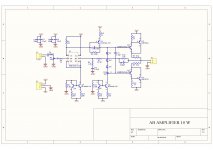
I also SIM this amp.
Attached you have sim to both version using others transistor models.
It also have some small changes - have a look on it and if possible compact your models files and upload it to make futhers tests with it
Regards
Attached you have sim to both version using others transistor models.
It also have some small changes - have a look on it and if possible compact your models files and upload it to make futhers tests with it
Regards
Attachments
60% signal reduction to amplify again...I know tail pair is not well balanced, R21 and R10 are in the real a 25K trimmer, set to get R10=22.7K and R21=3.3K...
R13+R17 are 100 ohm trimmer, to adjust bias current, also here not the best implementation.
Omit R17 as it does nothing in the circuit; if the trimmer is reduced to 25Ω R17 is shorted (0Ω) bij the wiper and layout.
I think the current mirrors Q8-Q9 and Q5-Q11 are fighting each other.
Change in value of diff current from Q8-Q9 sets Q10 on a different setting too, but might not correspond with the actual current from Q5-Q11. If the difference is to large to handle by the feedback, the output has no other escape than a hanging to a rail.
If R1 is really 474 ohms there is not enough current in the LTP?
Input resistances ought to be balanced, not sure why R21 is so high - it's attenuating the gain.
Check the currents in the LTP and VAS - seems a little unbalanced from what I can see.
Input resistances ought to be balanced, not sure why R21 is so high - it's attenuating the gain.
Check the currents in the LTP and VAS - seems a little unbalanced from what I can see.
Attached there are spice files and simulation.
Tail current is 3.5mA, VAS current 5 mA. Not balanced?
I know input resistance is not well balanced, I'll do it in the next rev of the amp. Anyway the problem should be somewhere else.
I don't understand the comment about current mirrors are fighting each other
Tail current is 3.5mA, VAS current 5 mA. Not balanced?
I know input resistance is not well balanced, I'll do it in the next rev of the amp. Anyway the problem should be somewhere else.
I don't understand the comment about current mirrors are fighting each other
Simulations are a representation of the reality. The reality however does not correspond with simulations (or personal perspectives). The idealised simu's can work, but the real semiconductors behave somewhat different and with generous amount of variation of specifications. Hence the simu is ok and the thing itself unstable....but the simulation is really fine so I don't understand why.
No, not 'not balanced?', but not immidiate related, only through Q10.Tail current is 3.5mA, VAS current 5 mA. Not balanced? ... Anyway the problem should be somewhere else.
It is the very reason of the dc-instability (Q10-Q11 fight). Follow the hints from #4 and #14.I don't understand the comment about current mirrors are fighting each other
Attached there are spice files and simulation.
Tail current is 3.5mA, VAS current 5 mA. Not balanced?
I know input resistance is not well balanced, I'll do it in the next rev of the amp. Anyway the problem should be somewhere else.
I don't understand the comment about current mirrors are fighting each other
Dear mtx489,
You open this thread asking detail related to DC instability.
I found 2 schematics in the net with lots of basic errors. I suppose the idea was show the current mirror advantage in the first stage. In my simulations files I show the THD result of both schematics.
You asked about relation between first stage and second stage here.
The first stage current defines almost all amplifier parameter as THD, frequency response and slew rate. It is related with the impedance load from second stage. The second stage has impedance which can be seen as a load resistance and a very variable capacitance. The first stage current must charge this capacitance to define slew rate and directly the frequency response from amplifier. Here you can see the importance of the first stage current. If you apply current mirrors in first stage, you will find a best THD figure as you can see in my SIM Files. For DC offset you must care the base current in bipolar transistor from first with equal resistance seen from both BJT
The second stage current is main related to thirty stage current. It must be defined to balance both stage (first and output) in such way to find the best overall amplifier behavior. I mean THD and step response.
To validate you have a good project the step response or square wave response will show you if all is really OK with a perfect square wave over a load. Resistive ou complex as I show in my simulation file.
In my SIM I corrected all the first stage errors that created a poor frequency response and a big DC error in output.
Regards and Be Safe
Ronaldo
Attachments

Last edited:
C9 is still a bit low, for the value of the resistor. A 30 Hz corner freq? That should be more like 3 Hz unless you don’t like bass. And C6 is way too low too. If you use a pF range cap at the input, it would be in shunt to roll off any RF, not as a DC block. That cap should be increased to pass 20 Hz as well. You will figure that out quickly just by listening.
In general those poles do not affect low frequency stability. But they do affect how to behaves when clipping at low frequency. It’s only a minor effect, but as a general rule the input coupling cap should set the LF roll off. It does now, but it’s way too high with 330 pF. The feedback cap should be the next corner frequency, and the pole frequency set by the power supply cap and the *load* should be the lowest. That’s not always practical or extremely critical, but does give the best overall result when you start building extremely high performance amplifiers. It will produce the best-looking “tops” of the waveform when clipping at less than 120 Hz.
Low frequency instability in solid state amps is almost always as the above have posted - problems with offsets and thermal time constants fighting each other. The only way to simulate it is with a full electro-thermal model. Just using best practices will get rid of it.
And short pins 2 and 3 of R16 (bias pot). An open wiper can take out the output stage if it is not constrained.
In the sim V5 is wrong polarity. You have +ve going to -ve rail.
Other than that only thing that seems unusual is current mirrors to provide a constant current source. But should work.
Maybe try higher C3 maybe 100pf ?
R18 is pretty much redundant.
Other than that only thing that seems unusual is current mirrors to provide a constant current source. But should work.
Maybe try higher C3 maybe 100pf ?
R18 is pretty much redundant.
- Home
- Amplifiers
- Solid State
- AB amplifier DC instability