LOL, you post a simple circuit and everybody takes shots at improving it whether you ask for it or not 😀
Since we're talking versatility, shouldn't we pick a transistor with higher Vce? TIP50 is only 400V. And some of the high(er) voltage ones come with a built-in diode.
We could but whats the point ? I state that the biggest smart differential voltage youll see on the the entire contraption is 200V. So it means you can regulate 200V from 400V or 400V from 600V. Either way anythign more will just not be a smart move. Also the LR8 is limited to 400someodd V..less than 450V. So really there is no point.
We could but whats the point ? I state that the biggest smart differential voltage youll see on the the entire contraption is 200V. So it means you can regulate 200V from 400V or 400V from 600V. Either way anythign more will just not be a smart move. Also the LR8 is limited to 400someodd V..less than 450V. So really there is no point.
The LR8 is limited to Vin-Vout of 450V. I was thinking of having at least the same standoff for the transistor, for momentary fault/transient reasons. And a reverse diode for the same reason. No I wasn't planning on dropping 400V across the transistor in steady state, although interestingly the second example in the LR8 data sheet shows it's ok to drop 445V across it.
No sane person will regulate 400 to 200V or 600 to 400V 😀 I hope ...
That will come as news to Keithley, Fluke Mfg, Keysight (nee Hewlett Packard) and a host of others.
This regulator is useful for regulating pentode G2 , and it is very sane 😀 ... If the voltage drop is very high a series power resistor should be added .
I guess it depends on what you mean by deterioration and what is connected to the output, particularly what types and values of decoupling capacitors. With decoupled ADJ pin, you have much more high-frequency loop gain which makes the regulator more prone to ringing, but when you manage to keep that under control, you will also have much faster settling after a load step than without ADJ decoupling.
TI brought it up in a technical note after Nat Semi wrote an article on LM317 noise reduction! I haven't seen it as an issue.
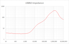
I can do some tests on the LR8N -- Zout, transient response, noise spectrum
Finally we agree on something 😉 Good night!
Here to satisfy you 😎 😀
Also having the option to run either full bridge or full wave via two diodes and a CT (commonly seen in radios with vacuum diodes or amps for that matter) with a smart sized heatsink 4X RAD-DY-KY/3 Heatsink: moulded TO220,TO247 black L: Amazon.co.uk: Electronics
Edit: Yes I am aware that the mounting is awkward and Ill problably change that
Attachments
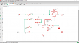
Instead of including extra diodes or the provision for them, you could use a jumper between B and D5 and one to disconnect the bottom diodes to switch between bridge and full wave 🙂 just a thought.
Last edited:
Instead of including extra diodes or the provision for them, you could use a jumper between B and D5 and one to disconnect the bottom diodes to switch between bridge and full wave just a thought.
Just gotta be real careful with that jumper.
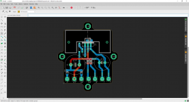
If it's a first time w HV, there are some tutorials on PCB layout for these voltages. You have to be careful with trace separation, eliminate the possibility of getting a finger in the wrong place, etc, etc.
Exactly why I use design rules in eagle. Yes I admit i may have overdone the diode separation in the bridge rectifier. Two diodes are actually on top of each other so you I get to join on side of them dogether with a via from top to bottom and then connect then on their own layer so it will turn out to be + on the top and - on the bottom layer. I have already pulled the diodes a bit further apart. Above all I dont manufacture PCBs at home anymore, so I get to have nice things like soldermask and use its dielectric capabillities to my advantage
Instead of including extra diodes or the provision for them, you could use a jumper between B and D5 and one to disconnect the bottom diodes to switch between bridge and full wave 🙂 just a thought.
I think the safer bet would be just not solder all the diodes. I dont mind the pads there when left unused. Lets say I would have a radio that had a bridge rectifier and one with a tube rectifier. Well I would solder the 4 diodes in their position for the bridge rectiffied one and I would solder only the two diodes for the radio that previously had a tube rectifier in. This way no confusion with jumpers will happen.
Here to satisfy you 😎 😀
Also having the option to run either full bridge or full wave via two diodes and a CT (commonly seen in radios with vacuum diodes or amps for that matter) with a smart sized heatsink 4X RAD-DY-KY/3 Heatsink: moulded TO220,TO247 black L: Amazon.co.uk: Electronics
Edit: Yes I am aware that the mounting is awkward and Ill problably change that
Not sure about this topology, the LR8 like the 317 works by providing a fixed voltage drop between the output terminal and the reference terminal, there is internal temperature compensation that maintains that voltage differential as relatively constant, now you've added about 700mv to that (pass transistor Vbe) which has an uncompensated TC of about 10mV/°C, that is going to result I think (and I could be wrong) in quite a lot of voltage drift due to varying operating temperature of the transistor. (And the drift is scaled by the ratio of your feedback resistors.)
In my implementations I use the LR8 as suggested in the data sheet, use an LPF filter to filter out the not insignificant noise in the output of this device and feed it to an IRF820 which is the pass element. It's quiet, works well and has been reliable over the 4 years or so I have been using this topology. Output impedance is low (determined by the transconductance of the mosfet you choose) and I shunt the source with 22uF - 47uF to ground.
X axis frequency, Y axis impedance?
No its actually two pi radians per second. the Y axis is Joules per second.
- Home
- Amplifiers
- Tubes / Valves
- Regulating high voltage (up to 450V) has become as easy as a LM317!