I guess you mean Q6 Patrick, not Q8 ?
There should be 12 volts between R12 and R20.
Maybe R17 are open.
Figge
Hi, Figge
I really mean Q8 maybe B/E shorted and need to check.
I think the amp's input fets and some other transistors failed together, it need more voltages measurement and replace parts to fix it.
Those input fets each pair with 35mA current is too high and Q6 base voltage is not so good, but if R17 open then R16 will pull the base voltage to the 24v rail.
I see now what you mean Patrick.
It would have been nice with some more measurements to check where the currents flow.
If there's a large offset on output one can be fooled when it turns IPS currents upside down, so maybe one could disconnect the outputstage to isolate the problem.
BR
Figge
It would have been nice with some more measurements to check where the currents flow.
If there's a large offset on output one can be fooled when it turns IPS currents upside down, so maybe one could disconnect the outputstage to isolate the problem.
BR
Figge
OK guys,I see now what you mean Patrick.
It would have been nice with some more measurements to check where the currents flow.
If there's a large offset on output one can be fooled when it turns IPS currents upside down, so maybe one could disconnect the outputstage to isolate the problem.
BR
Figge
I did lots of measurements today, and I will do more tomorrow. I have work I have to tend to for now, but I will post a much more complete picture with many voltages and currents. It does seem tricky, but I think we're getting close.
Once again I thank you for your input.
Ron
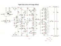
Here is the bad side with a bunch of voltages measured.
I will try to do the left side (good side) tomorrow for comparison.
Very puzzling to me at the moment. Notice the 4+ volts on the input!
I need to stop measuring and study instead for a while. I will try to do so tomorrow.
I don't think it's too difficult to disconnect from the OPS if that will help.
Thanks again for any input.
Ron
Attachments
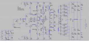
I made a simulation and disconnected the feedback and connected it to a voltage source that simulates 13V offset, wich results in similar readings that you've got.
So, if you disconnect the outputstage you will see if inputstage balances out.
There may be a broken mosfet or something in outputstage that pulls output high.
BR
Figge
So, if you disconnect the outputstage you will see if inputstage balances out.
There may be a broken mosfet or something in outputstage that pulls output high.
BR
Figge
Attachments
That's very helpful!I made a simulation and disconnected the feedback and connected it to a voltage source that simulates 13V offset, wich results in similar readings that you've got.
So, if you disconnect the outputstage you will see if inputstage balances out.
There may be a broken mosfet or something in outputstage that pulls output high.
BR
Figge
I will try it today, and if I see that the readings improve I will concentrate on the output stage.
Thank you very much.
Ron
Replace Q8, 9, 10, 11 and inspect the traces around those transistors for cracking or heat damage. If you look closely at the board you'll likely see discoloring in the area of those trans due to how hot they run. Typically they'll start failing by crackling & popping through the speakers. I replaced them in my 9300 years ago with the mpsa56w/06w transistors which are the 1W version.
Anyway this is a documented problem so I'd recommend replacing them first and then see where you stand after that. Even if they do not correct this problem they need to be replaced.
Anyway this is a documented problem so I'd recommend replacing them first and then see where you stand after that. Even if they do not correct this problem they need to be replaced.
Thanks.Replace Q8, 9, 10, 11 and inspect the traces around those transistors for cracking or heat damage. If you look closely at the board you'll likely see discoloring in the area of those trans due to how hot they run. Typically they'll start failing by crackling & popping through the speakers. I replaced them in my 9300 years ago with the mpsa56w/06w transistors which are the 1W version.
Anyway this is a documented problem so I'd recommend replacing them first and then see where you stand after that. Even if they do not correct this problem they need to be replaced.
I could not find the 1W version you speak of (there is no reference I find with a "W" at the end.) However I have ordered the 625mW versions. The bottom of the board is indeed discolored as you mentioned. I had attributed this to someone having already changed these out, but looking more closely I think these are indeed self burning--no soldering iron needed.
I will replace these as even with the measurements so far there is definitely something fishy about that line of transistors, as there are dV across them, but no current flow through some of them (c-e or e-c), even though they are highly biased. This is not true on the "good" side of the amp.
But while I wait if time permits I will disconnect the OPS from the IPS. There are problems on both sides, and it will be interesting to see which side heals once separated from the other side.
Ron
Thanks.
I could not find the 1W version you speak of (there is no reference I find with a "W" at the end.) However I have ordered the 625mW versions.
Sorry I was quoting off the top of my head and got it wrong as I normally do. The part numbers were MPSW56/06 and they were discontinued but arrow.com still shows some available. However the 625mW versions will probably outlast the amp at this point.
Here's a thread on this issue.
Q1 and Q2 are fets and the gates are very high impedance.
There should never be a dc voltage on them since they are grounded by R1 and R2.
Definitely there is a problem.
There should never be a dc voltage on them since they are grounded by R1 and R2.
Definitely there is a problem.
So strangely I'm not seeing voltages at the gates anymore, but everything else is still messed up. First I replaced Q8, Q9, Q10 and Q11. It didn't fix the offset.Q1 and Q2 are fets and the gates are very high impedance.
There should never be a dc voltage on them since they are grounded by R1 and R2.
Definitely there is a problem.
I then tried to isolate the output: I removed R32, R27 and R33. Still the IPS voltages were measuring similarly "bad" compared to the "good" side. I did notice a small current was flowing through R10, which wasn't the case before. At first the DC offset on the output was low, but I noticed it was slowly rising. Eventually it reached the prior level of ~12V.
I tried even disconnecting the +/- 70V at the rectifier output. The IPS voltages were still off in a similar way as before. The voltage across R16, for instance, was around 4V, making the gate voltages on Q1 and Q10 around 20V instead of 12V. The DC offset again rose slowly, but stabilized around 2V.
So I'm not sure if this means the problem is most likely in the IPS, i.e Q1 through Q6, or if it could still be in the OPS due to a bad output FET. I have some Exicon FET's which I think could work in the OPS, but I don't even want to try that if it's not likely going to fix the problem.
exact replacements for Q1 through Q4 are not obtainable as far as I know. Are there suitable substitutions available? And then they would need to be matched...I'm open to suggestions.
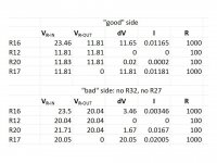
What I find strange is that the R16,17 voltage divider is not 1/2 the supply like it is on the other side
Rinman77, I don't see where you've measured the front end reg rail voltages (+/-24v). In my amp from several years ago it was running over +/- 29v and the 317/337 were hot as hell. Based on the divider voltage rsavas and others have mentioned it sounds like your voltage regs may be putting out a very high voltage.
This also puzzled me so I focused on this part of the circuit--here is what I found.What I find strange is that the R16,17 voltage divider is not 1/2 the supply like it is on the other side
Even my misbehaving amplifier must follow Ohm's law. I had measured R17 and determined its value was indeed very close to 1k. Likewise I measured the other side of R17 and it was 0V. Therefore we have current flowing to ground through R17 and R16 which should normally bring the gate voltage on Q9 and Q12 down to ~12V, as is measured on the "good" side, and as was also mentioned by Trollet in one of the first responses to my post. If current through R16 = current through R17, and R16=R17, and R16(in) = 24V, and R17(out)=0V, it follows that dV(R16) = dV(R17) AND dV(R16) + dV(R17) = 24V. Even though math isn't my strong subject it should follow dV=12 = gate voltage Q9 and Q12.
So where is the discrepancy? It is found in dV(R20) = 1.67V, where R10=100Ω. This gives I(R20) =16.7mA, thus most of the current through R17 is supplied from current flowing through Q10. This is where I'm over my head--I don't understand the nuances of transistor behavior under all circumstances. There must be current flow through the base of Q10. Based on the lack of dV across many of the resistors between Q9 and Q10, it is clear no current (or very little current) is flowing rail to rail through Q9, Q10, Q11, Q8. As a result there is no voltage drop across these transistors and resistors, which puts delta voltages of the wrong sign across some of the transistors. But it gets confusing trying to understand which problem is the source, and which is the result. The gate voltage on Q11 measures as expected, but the gate voltage on Q8 is way too negative (compared to the "good" side). This is also true at the other rail where the gate voltage on Q9 is too high due to insufficient current flow through R9. But what is causing the problem???😕
Trollet's simulation at this point becomes very interesting because he is able to get very similar results by adding a bad feedback voltage. But did I not sufficiently isolate the IPS with the removal of the resistors mentioned? It didn't seem to solve the problem in the IPS. So it seems it must be something related to Q1 through Q6, or maybe it is a result of something going on in the OPS, but the way it affecting the IPS is not clear. I am baffled.
See attached:So where is the discrepancy? It is found in dV(R20) = 1.67V, where R10=100Ω. This gives I(R20) =16.7mA, thus most of the current through R17 is supplied from current flowing through Q10.
Attachments
Looks to me that VAS-stage draws to much base current. As mentioned before it lives a tough life working hot with high current.
But I think it's a good idea to check Jfets to.
BR
Figge
But I think it's a good idea to check Jfets to.
BR
Figge
So strangely I'm not seeing voltages at the gates anymore, but everything else is still messed up. First I replaced Q8, Q9, Q10 and Q11. It didn't fix the offset.
I then tried to isolate the output: I removed R32, R27 and R33. Still the IPS voltages were measuring similarly "bad" compared to the "good" side. I did notice a small current was flowing through R10, which wasn't the case before. At first the DC offset on the output was low, but I noticed it was slowly rising. Eventually it reached the prior level of ~12V.
I tried even disconnecting the +/- 70V at the rectifier output. The IPS voltages were still off in a similar way as before. The voltage across R16, for instance, was around 4V, making the gate voltages on Q1 and Q10 around 20V instead of 12V. The DC offset again rose slowly, but stabilized around 2V.
So I'm not sure if this means the problem is most likely in the IPS, i.e Q1 through Q6, or if it could still be in the OPS due to a bad output FET. I have some Exicon FET's which I think could work in the OPS, but I don't even want to try that if it's not likely going to fix the problem.
exact replacements for Q1 through Q4 are not obtainable as far as I know. Are there suitable substitutions available? And then they would need to be matched...I'm open to suggestions.
Rinman,
I think that removing R27 wasn't a good idea. That left the feedback floating and may be why you measured a gradual rise in voltage. I believe that what you needed to do here in addition to removing R27 was to short across C7 or C9 which will give you a 1k ohm path to ground via R26 on the feedback side. You should also short the input RCA to ground. This will hold both sides of the
input LTP close to 0V.
I would also leave the output stage rail fuses out during this testing.
- Home
- Amplifiers
- Solid State
- Hafler Transnova 9300