Without the schematic posted, this thread will go on with endless specualation.
You have to take your clothes off at the doctor's office in order for them to know what's going on.
You have to take your clothes off at the doctor's office in order for them to know what's going on.
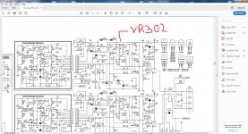
That VR302 looks to me to be a null/centering adjustment for the outputs, not a "bias" control.
In that situation, the adjustment is done to equalize the voltages between V+ and V- so they are equal at the speaker ouput.
More accurate results are done with an O scope and 1Khz sine wave at the beginning of clipping to balance things out.
In that situation, the adjustment is done to equalize the voltages between V+ and V- so they are equal at the speaker ouput.
More accurate results are done with an O scope and 1Khz sine wave at the beginning of clipping to balance things out.
Attached is a typical Vbe multiplier. The pot (rheostat) is normally installed at location R2. As you can see, as the value of R2 increases, the voltage at v (the amount of bias) decreases.
If R2 would totally fail and become an open circuit, v becomes 0.93 volts.
But the pot *could* be installed at R1, or it could replace both R1 and R2 with the wiper on the transistor base. But what I posted seems to be the most common, and is fail-safe.
This assumes the failure mode is open, however adjusting R2 to zero would be catastrophic, so R2 must include a fixed resistor in series that is the minimum R2 value and therefor a maximum vbe multiple. So there should be two fixed resistors in addition to the pot in a vbe multiplier. If the pot is in the R1 position then it is in parallel with a fixed resistor that sets a maximum resistance for R1.
That VR302 looks to me to be a null/centering adjustment for the outputs, not a "bias" control.
In that situation, the adjustment is done to equalize the voltages between V+ and V- so they are equal at the speaker ouput.
More accurate results are done with an O scope and 1Khz sine wave at the beginning of clipping to balance things out.
No. This is an interesting quasi-complimentary MOSFET output and VR302 is the bias adjustment. Bias increases with increasing resistance as VR302 is in the "R1" position.
The voltage between TP1 and TP2 is available to measure the bias current for one channel and TP3 and TP4 for the other. If you can not find a recommended value in the manual, my guess would be between 50mV and 100mV across these test points. It could be as much as 400mV (0.4V).
Posts 14,16,18 showed the service manual procedure for bias setting and the relevant schematic detail. Your doctor will diagnose OCD if you keep trying to take your clothes off when already naked 😀.Without the schematic posted, this thread will go on with endless specualation......
You guys are talking rocket science.
Original question.
How do I adjust the bias to minimum bias position. Do I set for maximum resistance for min bias or set for min resistance for min bias?
I was trying to see if there was a general rule for (blindly) adjusting the bias pot to set min safe bias.
Thanks guys!!
Original question.
How do I adjust the bias to minimum bias position. Do I set for maximum resistance for min bias or set for min resistance for min bias?
I was trying to see if there was a general rule for (blindly) adjusting the bias pot to set min safe bias.
Thanks guys!!
The simple answer, I'm afraid, is "no" [emoji16]You guys are talking rocket science.
Original question.
How do I adjust the bias to minimum bias position. Do I set for maximum resistance for min bias or set for min resistance for min bias?
I was trying to see if there was a general rule for (blindly) adjusting the bias pot to set min safe bias.
Thanks guys!!
Seems to me that the Service Manual would have the answers and information, as apposed to asking people on the internet.
We've seen the service manual advice and the specified bias current measurement but it says nothing about the direction or setting for minimum or maximum bias. Steveu has analysed the circuit and determined the wiper should be in the R1 position for maximum bias. Perhaps this is a typo because there's no R1 in this section of the amplifier and he means the RH position. This is the logical direction but let's see if he has a comment to add.
We've seen the service manual advice and the specified bias current measurement but it says nothing about the direction or setting for minimum or maximum bias. Steveu has analysed the circuit and determined the wiper should be in the R1 position for maximum bias. Perhaps this is a typo because there's no R1 in this section of the amplifier and he means the RH position. This is the logical direction but let's see if he has a comment to add.
I would rig up the amp on a dim bulb, then center the adjustment, then rotating it while measuring idle current.
That would clear up any questions, simple enough.
Thank you for all the contribution people but honestly I never thought it was going to be this difficult!!!! 😱😱😱😱😱
I mean the potentiometer varies something right?
The reason I am so keen because its eating me alive! I presumed that if I can understand one I will understand more. I know someone will now post never presume anything! 😀😀😀😀
I mean the potentiometer varies something right?
The reason I am so keen because its eating me alive! I presumed that if I can understand one I will understand more. I know someone will now post never presume anything! 😀😀😀😀
Shall we walk through a quick analysis?
Let's start out by making some assumptions:
1. The output, (C306 negative terminal), remains very near zero volts like a good little amplifier.
2. The drive from the connector pin 6 remains fixed. It won't but close enough for this analysis. (Just to put a number on it, say 2 volts.)
3. The bias feedback signal (Lbias) is working properly, but is of a small enough magnitude to ignore.
OK, let's continue:
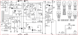
1. Q305, Q306 and the associated resistors form a Sziklai pair configured as a Vbe multiplier. 2. VR302 adjusts the voltage seen at the positive terminal of C306.
3. If we increase the resistance of VR302, the voltage at the positive terminal of C306 will increase so as to provide sufficient current to turn on Q306. Note there is no indication in the schematic if maximum resistance of the pot is fully CW or fully CCW. If you can find the circuit board layout, you may be able to determine it one way or the other.
4. When the voltage on the C306 increases, that increase will be seen by R309 and the emitter of Q304 increasing the emitter and hence the collector current.
5. An increase of the collector current of Q304 increases the voltage dropped across R315. This will pull the gate of Q308 closer the ground, increasing it's drain current. (since the source is connected to the negative rail)
Conclusion:
*Increasing* the resistance of VR302 *increases* bias current. Again, note that depending on how the part is configured on the board, maximum resistance might well occur when the pot is set fully CW. But then again it might not.
Let's start out by making some assumptions:
1. The output, (C306 negative terminal), remains very near zero volts like a good little amplifier.
2. The drive from the connector pin 6 remains fixed. It won't but close enough for this analysis. (Just to put a number on it, say 2 volts.)
3. The bias feedback signal (Lbias) is working properly, but is of a small enough magnitude to ignore.
OK, let's continue:
1. Q305, Q306 and the associated resistors form a Sziklai pair configured as a Vbe multiplier. 2. VR302 adjusts the voltage seen at the positive terminal of C306.
3. If we increase the resistance of VR302, the voltage at the positive terminal of C306 will increase so as to provide sufficient current to turn on Q306. Note there is no indication in the schematic if maximum resistance of the pot is fully CW or fully CCW. If you can find the circuit board layout, you may be able to determine it one way or the other.
4. When the voltage on the C306 increases, that increase will be seen by R309 and the emitter of Q304 increasing the emitter and hence the collector current.
5. An increase of the collector current of Q304 increases the voltage dropped across R315. This will pull the gate of Q308 closer the ground, increasing it's drain current. (since the source is connected to the negative rail)
Conclusion:
*Increasing* the resistance of VR302 *increases* bias current. Again, note that depending on how the part is configured on the board, maximum resistance might well occur when the pot is set fully CW. But then again it might not.
Attachments
Last edited:
😕😕😕😕 Do I set the boas to maximum resistance or lowest then to get minimum bias?
For the 100th time: that question can not be answered until you post the proper schematic.
Whay is that simple truth so hard to understand for you? 😕😕😕
YOU are being incredibly stubborn and difficult about NOT doing your homework and instead begging/pushing/screaming for an impossible answer.I never thought it was going to be this difficult!!!!
Last edited:
a good way to start would be to know that:
1. tubes are normally conducting with zero grid bias, so that a resistor placed at the cathode ensures the grid is in negative voltage bias territory, a grid leak resistor to ground is mandatory...
2 bipolar transistors are normally off devices, you have to inject base current to get the collector current to conduct....jfets too...
3. enhancement mosfets are also normally non conducting...whereas depletion mosfets are like tubes in that they are normally conducting drain currents....
so with this you can start your own journey in the business of biasing...
Shall we walk through a quick analysis?
Let's start out by making some assumptions:
1. The output, (C306 negative terminal), remains very near zero volts like a good little amplifier.
2. The drive from the connector pin 6 remains fixed. It won't but close enough for this analysis. (Just to put a number on it, say 2 volts.)
3. The bias feedback signal (Lbias) is working properly, but is of a small enough magnitude to ignore.
OK, let's continue:
1. Q305, Q306 and the associated resistors form a Sziklai pair configured as a Vbe multiplier. 2. VR302 adjusts the voltage seen at the positive terminal of C306.
3. If we increase the resistance of VR302, the voltage at the positive terminal of C306 will increase so as to provide sufficient current to turn on Q306. Note there is no indication in the schematic if maximum resistance of the pot is fully CW or fully CCW. If you can find the circuit board layout, you may be able to determine it one way or the other.
4. When the voltage on the C306 increases, that increase will be seen by R309 and the emitter of Q304 increasing the emitter and hence the collector current.
5. An increase of the collector current of Q304 increases the voltage dropped across R315. This will pull the gate of Q308 closer the ground, increasing it's drain current. (since the source is connected to the negative rail)
Conclusion:
*Increasing* the resistance of VR302 *increases* bias current. Again, note that depending on how the part is configured on the board, maximum resistance might well occur when the pot is set fully CW. But then again it might not.
Thank you for this break down!
For the 100th time: that question can not be answered until you post the proper schematic.
Whay is that simple truth so hard to understand for you? 😕😕😕
YOU are being incredibly stubborn and difficult about NOT doing your homework and instead begging/pushing/screaming for an impossible answer.
I cannot seem to attach the schematic but it can be downloaded here
NAD C300 - Manual - Stereo Integrated Amplifier - HiFi Engine
Just go to post #15 and look at the parts overlay for the PCB. That's where you see which end of the pot is common with the wiper and identifies which way the pot should be rotated to increase or decrease resistance. Is it so hard for everyone to scan the thread fully, click on the thumbnail and see that the OP already supplied the information?Shall we walk through a quick analysis?.......................
3. If we increase the resistance of VR302, the voltage at the positive terminal of C306 will increase so as to provide sufficient current to turn on Q306. Note there is no indication in the schematic if maximum resistance of the pot is fully CW or fully CCW. If you can find the circuit board layout, you may be able to determine it one way or the other................*Increasing* the resistance of VR302 *increases* bias current. Again, note that depending on how the part is configured on the board, maximum resistance might well occur when the pot is set fully CW. But then again it might not.
Link to the manual, free sign up and download: NAD C300 - Manual - Stereo Integrated Amplifier - HiFi Engine

It appears to me that minimum resistance, and therefore minimum bias will occur with the pot fully CW.
BUT YOU DON"T WANT TO TAKE THAT AS GOSPEL. Leave the adjustment where it is, power up the unit, and measure the voltage across the 2 ohm sense resistor. Higher voltage = higher current. Including a DBT on the line input is usually a good idea too.
BUT YOU DON"T WANT TO TAKE THAT AS GOSPEL. Leave the adjustment where it is, power up the unit, and measure the voltage across the 2 ohm sense resistor. Higher voltage = higher current. Including a DBT on the line input is usually a good idea too.
- Status
- Not open for further replies.
- Home
- Amplifiers
- Solid State
- resistors and Bias