Thinking about Dick Moore's notch filter and how he enjoyed working with the Heathkit IG-18 seems it would be a natural fit to use the IG's chassis and switches to build a notch filter with tens, units, variable tenths, and multiplier for frequency control as already laid out on the front panel.
That was a fun read! Thank you to Michael K. and to Bob C. for posting it.
It amused me to see {caption of Figure 8} that he found the uncompensated 2T current source's phase margin to be 28 degrees, vigorously in agreement with my phase margin results (26 & 27 degrees) in post #7772. And completely at odds with the quoted passage in post 7769.
Installing the new R and the new C brings the parts count up to 6 devices per current source, whereas the ZD+2R+T CCS needs only 4 devices and Camille's Cascode has 6 devices. This one does have other advantages, as Michael points out. But "fewer parts" is no longer one of them.
Interesting article, which seems to confirm that a 1k resistor into the control transistor's base gives sufficient phase margin. Incidentally that value seen in most schematics, so it probably works well in practice.
Two unanswered questions directed to those here with the necessary knowledge and skills:
1) How does inserting 10R into the control transistor's emitter improve on the basic circuit?
2) Is the ~1k ohm resistor suggested by Bob to isolate the CCS from the low impedance LTP really necessary if these other measures are taken care of?
Finally I think I have posted Michael's ANF current source article successfully. I posted the article in 2 pdf pieces. I apologize for the delay and thank all of those who posted suggestions. I am such a computer Geek - NOT!
Cheers,
Bob
I took the liberty of downloading/merging/uploading 🙂
It is easy to merger/shrink the pdf using iLovePDF | Online PDF tools for PDF lovers
Attachments
I would like to thank Robert Cordell for the interesting article. For me the most important lesson:Finally I think I have posted Michael's ANF current source article successfully. I posted the article in 2 pdf pieces. I apologize for the delay and thank all of those who posted suggestions. I am such a computer Geek - NOT!
Cheers,
Bob
This is one of those grains of gold, for them I came here.The output impedance of the ANF current source is superior to that of the voltage-reference-biased current source across the audio band.
Thank You, Bob.
Last edited:
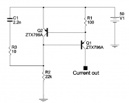
Bob, I've been thinking about what you might say in your 2nd edition, regarding Michael Kiwanuka's modified current source circuit. I've wondered what might be a simple and robust design procedure for choosing the values of his frequency compensation components R3 and C1 (schematic below).
One design algorithm for choosing R3 and C1, which does give a robustly stable circuit, is the following:
_
One design algorithm for choosing R3 and C1, which does give a robustly stable circuit, is the following:
1. Put the circuit into LTSPICE (omitting C1 and R3), and run an AC analysis simulation. Find the magnitude of the open loop transfer function at a very low frequency like 100Hz. Call this number LFGAINDB. Also find the frequency at which the open loop transfer function has fallen 3dB below LFGAINDB, i.e., the dominant pole frequency. Call this number DPBEFORE.
2. Calculate the impedance at the collector of the control transistor Q2. This is roughly equal to (R1 * BetaQ1) // R2. Call this number ZCOLL.
3. Choose C1 such that ZCOLL and C1 form a pole at a frequency 100X lower than DPBEFORE. Numerically,
4. Choose R3 such that R3 and C1 form a zero at 2X the new unity gain crossover. Numerically,
5. Install R3 and C1 into the LTSPICE simulation and assign them the values calculated in steps 3 and 4. Simulate again and verify that the phase margin and gain margin are acceptable.
However, the above might be an intimidating amount of simulation and arithmetic for some of your readers. Maybe you can streamline and simplify it a bit? A guideline or rule-of-thumb that doesn't involve LTSPICE simulations would be a great delight to many readers. 2. Calculate the impedance at the collector of the control transistor Q2. This is roughly equal to (R1 * BetaQ1) // R2. Call this number ZCOLL.
3. Choose C1 such that ZCOLL and C1 form a pole at a frequency 100X lower than DPBEFORE. Numerically,
C1 = 100 / (ZCOLL * 2 * PI * DPBEFORE)
4. Choose R3 such that R3 and C1 form a zero at 2X the new unity gain crossover. Numerically,
DPAFTER = DPBEFORE / 100
LFGAINX = ANTILOG10(LFGAINDB / 20)
UGCNEW = DPAFTER * LFGAINX
R3 = 1 / (4 * C1 * PI * UGCNEW)
LFGAINX = ANTILOG10(LFGAINDB / 20)
UGCNEW = DPAFTER * LFGAINX
R3 = 1 / (4 * C1 * PI * UGCNEW)
5. Install R3 and C1 into the LTSPICE simulation and assign them the values calculated in steps 3 and 4. Simulate again and verify that the phase margin and gain margin are acceptable.
_
Attachments
Interesting article, which seems to confirm that a 1k resistor into the control transistor's base gives sufficient phase margin. Incidentally that value seen in most schematics, so it probably works well in practice.
Two unanswered questions directed to those here with the necessary knowledge and skills:
1) How does inserting 10R into the control transistor's emitter improve on the basic circuit?
2) Is the ~1k ohm resistor suggested by Bob to isolate the CCS from the low impedance LTP really necessary if these other measures are taken care of?
1) I'm guessing that it has to do with the reduction of transconductance of the control transistor, but that angle might not make much sense for cases where that transistor is operated at increasingly lower currents, like, say, 500uA, where re' is already up to about 52 ohms. Of course, the 10 ohms value can be increased to keep its ratio to re' about the same.
2) The main reason that I like to use the 1k (or greater) isolation resistor in the tail is to provide some isolation from the output capacitance of the CCS, thinking that common mode effects from EMI might be reduced. If you have 2 mA tail and 50V rails, you can afford to use a value as high as 10k or more, since you have headroom to burn for the CCS. This also can reduce dissipation in the CCS transistor.
Cheers,
Bob
mark:
i don't remember if i've made this comment before to you, but i often feel a small electronics book in you is slowly trying to sneak out!
maybe you should go ahead and let it ...
🙂
mlloyd1
(in case i need to be more blunt, thanks for the "analytical" explanations.)
i don't remember if i've made this comment before to you, but i often feel a small electronics book in you is slowly trying to sneak out!
maybe you should go ahead and let it ...
🙂
mlloyd1
(in case i need to be more blunt, thanks for the "analytical" explanations.)
Thanks but my friend Tom (author of these books) tells me that the hourly wage is very low.
Summation_from_t=0_to_t=infinity(Royalty dollars) / Summation(Hours spent)
is a discouragingly small number.
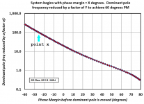
edit- here's a complete non-sequitur (attached below). Point x represents my opinion of the worst case starting point (-25 degrees of Phase Margin, i.e., guaranteed oscillation). If you lower the dominant pole by 100X, Phase Margin becomes +60 degrees. Much more better. That's where "100X" came from in step 3 of the design algorithm.
_
Summation_from_t=0_to_t=infinity(Royalty dollars) / Summation(Hours spent)
is a discouragingly small number.
edit- here's a complete non-sequitur (attached below). Point x represents my opinion of the worst case starting point (-25 degrees of Phase Margin, i.e., guaranteed oscillation). If you lower the dominant pole by 100X, Phase Margin becomes +60 degrees. Much more better. That's where "100X" came from in step 3 of the design algorithm.
_
Attachments
Last edited:
Is it possible to just bypass the publisher/amazon and sell yourself online? I mean selling an encryption key for a pdf file? just thinking of a way to take out the middle man that steals all the profit.Thanks but my friend Tom (author of these books) tells me that the hourly wage is very low.
Thanks Bob, even though I haven't had any ill-effects without, I'm going back to using the 1k Rb just to be on the safe side. Cheap insurance if you will. I'll also try that resistor between the CCS and LTP as you suggest 
I mean selling an encryption key for a pdf file?
Ask Bob about that, it ends up at some .ru site for free. The rub is compressed I think Bob's whole book was only a 5 Meg download.
Thanks but my friend Tom (author of these books) tells me that the hourly wage is very low.
Summation_from_t=0_to_t=infinity(Royalty dollars) / Summation(Hours spent)
is a discouragingly small number.
edit- here's a complete non-sequitur (attached below). Point x represents my opinion of the worst case starting point (-25 degrees of Phase Margin, i.e., guaranteed oscillation). If you lower the dominant pole by 100X, Phase Margin becomes +60 degrees. Much more better. That's where "100X" came from in step 3 of the design algorithm.
_
Hi Mark,
I can assure you that you are correct in regard to royalties vs effort 🙂
Cheers,
Bob
edit- here's a complete non-sequitur (attached below). Point x represents my opinion of the worst case starting point (-25 degrees of Phase Margin, i.e., guaranteed oscillation). If you lower the dominant pole by 100X, Phase Margin becomes +60 degrees. Much more better. That's where "100X" came from in step 3 of the design algorithm.
_
So this reminds me of a question that's been bugging me for some time. So one 'classical' measurement of stability is to drive the amp with a square wave, stick a cap load at the other end and look for ringing/overshoot. There are nice nomograms that translate the degree of overshoot into PM.
So far, so good. The problem in practice though is that real world big power amps have stray inductances. And so you can have an amp with 60 degrees pm that would show overshoot on the test above. Even those that model well and have the op inductor removed- all just due to strays.
So after that long context setting, here's the question:
How do you tell if the ringing of an amp driving a cap is due to: a)insufficient phase margin or b) presence of parasitic inductances.
Bob, I've been thinking about what you might say in your 2nd edition, regarding Michael Kiwanuka's modified current source circuit. I've wondered what might be a simple and robust design procedure for choosing the values of his frequency compensation components R3 and C1 (schematic below).
One design algorithm for choosing R3 and C1, which does give a robustly stable circuit, is the following:1. Put the circuit into LTSPICE (omitting C1 and R3), and run an AC analysis simulation. Find the magnitude of the open loop transfer function at a very low frequency like 100Hz. Call this number LFGAINDB. Also find the frequency at which the open loop transfer function has fallen 3dB below LFGAINDB, i.e., the dominant pole frequency. Call this number DPBEFORE.However, the above might be an intimidating amount of simulation and arithmetic for some of your readers. Maybe you can streamline and simplify it a bit? A guideline or rule-of-thumb that doesn't involve LTSPICE simulations would be a great delight to many readers.
2. Calculate the impedance at the collector of the control transistor Q2. This is roughly equal to (R1 * BetaQ1) // R2. Call this number ZCOLL.
3. Choose C1 such that ZCOLL and C1 form a pole at a frequency 100X lower than DPBEFORE. Numerically,
C1 = 100 / (ZCOLL * 2 * PI * DPBEFORE)
4. Choose R3 such that R3 and C1 form a zero at 2X the new unity gain crossover. Numerically,
DPAFTER = DPBEFORE / 100
LFGAINX = ANTILOG10(LFGAINDB / 20)
UGCNEW = DPAFTER * LFGAINX
R3 = 1 / (4 * C1 * PI * UGCNEW)
5. Install R3 and C1 into the LTSPICE simulation and assign them the values calculated in steps 3 and 4. Simulate again and verify that the phase margin and gain margin are acceptable.
_
Hi Mark,
Thanks. I think that some kind of simplified guideline would be quite useful. Putting in a >1k base resistor is probably safe, but I like the idea of putting in some simple lag-lead compensation as shown, when necessary. Not sure if there are any disadvantages in taking the easy way out, but it may be worth a look.
The first guideline would be to not allow any significant capacitance, stray or otherwise, across the emitter resistor of the current source transistor and keep the layout compact. I think you have to work to get more than 5pF of stray there. When the collector of the current source transistor is terminated in a very low impedance, that transistor devolves into an emitter follower. If there is, say, 30 pF across the emitter resistor, we begin to get into the zone of emitter follower instability and negative resistance looking into the base of that transistor.
I also suspect that control transistors with high internal base resistance may be more prone to reduced phase margin. Maybe a transistor like a 2N4401/4403, with very low Rbb will result in a stable 2T CCS virtually all of the time. I'll try a sim of it.
Of course, it would be nice to have a guideline that indicates that the 2T CCS is safe in its native, uncompensated form, as it may be in many circuit environments.
Cheers,
Bob
Is it possible to just bypass the publisher/amazon and sell yourself online? I mean selling an encryption key for a pdf file? just thinking of a way to take out the middle man that steals all the profit.
You really need to be on Amazon to sell books. No longer do you need to be in Brick-and-Mortar. You also do not necessarily need a large traditional publisher to publish a book and get it onto Amazon. Outskirts Press, CreateSpace and many others can do that for you, and the $/book in royalties you get back is a bigger fraction of the book selling price. The biggest innovation in publishing that has opened up these possibilities is POD (print-on-demand), as opposed to the traditional need to set up and do a big print run. This is especially significant for technical books, where you are not going to be selling 100,000 copies.
I'm sure Jan could say a lot more about all of this, given his deep publishing experience with LA.
That having been said, the publishers do an awful lot of heavy lifting to get a book published from a mere manuscript submitted by an author. I am quite certain that my book would never have come into existence without my traditional publisher.
If you author a technical book, don't quit your day job. We are not talking 50 Shades of Grey here 🙂.
Cheers,
Bob
The first guideline would be to not allow any significant capacitance, stray or otherwise, across the emitter resistor of the current source transistor and keep the layout compact.
Hi Bob, do you have any specific recommendations other than to keep the layout compact? I use 0805 resistors in the CCS, SOT-23 for the control Q and either a TO-92 or TO-126 for the pass device, depending on the usage. The whole sub-circuit is very compact, with all traces 1/2 inch or less, with the exception of the power in and current out traces. I normally bypass the rail with a 100n X7R within 2 inches of the CCS. I've never had any problems attributed to the CCS even when Rb is left out. Parts typically BC857 (control Q) and KSA992/1381 (pass Q).
The first guideline would be to not allow any significant capacitance, stray or otherwise, across the emitter resistor of the current source transistor and keep the layout compact.
I also suspect that control transistors with high internal base resistance may be more prone to reduced phase margin. Maybe a transistor like a 2N4401/4403, with very low Rbb will result in a stable 2T CCS virtually all of the time. I'll try a sim of it.
- Self inductance of the transistor pins (up to 15 nH) doesn't make much difference.
- The impedance of the load driven by the current source is critical. Lower impedance loads (such as the emitters of an LTP) result in MUCH worse phase margin.
- The ratio of currents between the two transistors doesn't make much difference.
- Stray capacitance across the current sense resistor ("R1" in the schematic below) can destroy phase margin.
- Different transistor part#s (i.e. different SPICE model parameters) gave different amounts of phase margin. The Fairchild KSA992 (model supplied by Linear Technology) was worst among the PNPs I tried. The BC560C (model supplied by Cordell Audio) was second worst; it needed 30pF of stray cap to begin oscillating.
I think it would be a surprise if reducing the transistor's internal base resistance rbb turns out to improve stability, since both folklore and simulation agree that *adding* 2K of base resistance externally does improve stability.
Michael Kiwanuka's conjecture that there may be a single set of values for the RC compensator in his 6-device current source, which guarantee stability for ALL possible choices of transistor types, resistor values, supply voltages, and output currents ... might turn out to be correct or mostly-correct. Perhaps a Universally Stable design unavoidably sacrifices a lot of performance at high frequencies, in exchange for guaranteed stability. But maybe that's okay with lots of your readers.
A grad student could bang out the simulations needed to verify universal stability, in less than a week. Treat it as a "PVT corners" type of exercise where you explore all possible combinations of (i) max and min Beta; (ii) max and min VA; (iii) max and min rbb; (iv) max and min fT; (v) max and min Cbc; (vi) max and min Iout; (vii) max and min Cstray.
That's only 2^7 = 128 simulations, a finite number. But I'm not volunteering to build or run them myself!
Hi Bob, do you have any specific recommendations other than to keep the layout compact? I use 0805 resistors in the CCS, SOT-23 for the control Q and either a TO-92 or TO-126 for the pass device, depending on the usage. The whole sub-circuit is very compact, with all traces 1/2 inch or less, with the exception of the power in and current out traces. I normally bypass the rail with a 100n X7R within 2 inches of the CCS. I've never had any problems attributed to the CCS even when Rb is left out. Parts typically BC857 (control Q) and KSA992/1381 (pass Q).
This sounds like a very good, tight layout. I would guess the parasitic capacitance across the emitter resistor would be less than 2pF at most. I don't have a model for the BC857, so can't simulate it. Sometimes I have put a light Zobel network shunting the VAS output node to ground to keep the impedance on that node a little more real for better phase margin, and that may also add some stability to the 2T CCS, helping to keep that node from looking inductive. I usually use 47pF and 100 ohms in series.
As noted earlier in this thread, the stability of the 2T CCS depends heavily on the nature of its load in the actual application, with a zero-impedance load appearing to be one of the worst cases. In an amplifier with a single-ended VAS and Miller compensation, the load is quite different and more complex, especially due to the Miller compensation feedback loop around the 2T VAS. I can't say if such a load on the 2T CCS makes stability better or worse. An ideal Miller-compensated VAS would present a very low node impedance at high frequencies as a result of its shunt feedback. However, as with any negative shunt feedback circuit, the impedance will generally begin to rise at some high frequency, making it look somewhat inductive.
This may be an example where poking the VAS+CCS circuit with a pulse in simulation and looking at the ringing might be the best way to evaluate the local stability of the VAS + CCS load.
This could be done in simulation by stabiilizing the circuit in open-loop with a dc servo function, then poking the VAS output node with a fast current pulse of value perhaps 10% of the VAS bias current. Just thinking out loud here.
Cheers,
Bob
- Home
- Amplifiers
- Solid State
- Bob Cordell's Power amplifier book