The guidance above is appropriate for two of the 12 grounds in this system, optionally four. For the other eight it'll degrade performance to some extent. Be careful also of focusing on ground to the exclusion of other power delivery nets.Is that correct?
The grounding article in (surprise! 😛) the articles section goes through the relevant concepts at some length.
The guidance above is appropriate for two of the 12 grounds in this system, optionally four. For the other eight it'll degrade performance to some extent. Be careful also of focusing on ground to the exclusion of other power delivery nets.
The grounding article in (surprise! 😛) the articles section goes through the relevant concepts at some length.
Can anyone translate that? I can't!
@rayma: I've made some progress following your advice. I rearranged the circuit layout (only the components around the op amp in the upper right corner) to move the feedback cap close to the pins, and moved some parts around. Mostly finished there. Still have to do the same around the op amp at bottom right.
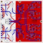
I also put in a ground plane as you suggested, including the final PS caps and the regulator circuitry.
Please see layout, attached. Circuit remains the same as in post 1.
I also put in a ground plane as you suggested, including the final PS caps and the regulator circuitry.
Please see layout, attached. Circuit remains the same as in post 1.
Attachments
I also put in a ground plane as you suggested, including the final PS caps and the regulator circuitry.
Looks better. See how simplified the layout is when you use the ground plane? For smt it would be the top layer.
Keep in mind that you want to make connections to high impedance nodes (inverting pin of op amp) compact,
and also use component placement to reduce trace lengths in general.
Looks better. See how simplified the layout is when you use the ground plane? For smt it would be the top layer.
Keep in mind that you want to make connections to high impedance nodes (inverting pin of op amp) compact,
and also use component placement to reduce trace lengths in general.
Great! I really appreciate that you took the time to give me some advice that was specific enough for me to know what to change. I'll keep working on the layout over the next couple of days.
I would still like to hear from other voices. Please be specific in your comments so that I can understand what exactly would improve the layout, etc. Thanks.
At this point I have finished the new layout with the ground plane. Then I thought about how this could be made more user friendly. How about RCA connectors for all the inputs and outputs?
I loaded up a model of this jack (WBTOR1):

http://datasheet.octopart.com/WBTOR1-Lumberg-datasheet-13036254.pdf
(sorry, it's the only one that comes with my layout program).
Based on the footprint of the jack I can fit eight of these along the side of the board where the inputs and outputs are located. This would make the board more user friendly for some, and for those who don't want the extra cost for the jacks ($2 each), you can just solder the input and output wires into the proper holes (marked T and S).
See attached layout screen shot with the jack positioned along the board edge, along the side of the board where they would be located. In order to accommodate the jacks on the PCB I will need to move the active circuit section to the left a bit, and squeeze some other components together (e.g. in the PS section). It's totally doable.
Do you think that including the RCA jacks would be worthwhile?
.
I loaded up a model of this jack (WBTOR1):
http://datasheet.octopart.com/WBTOR1-Lumberg-datasheet-13036254.pdf
(sorry, it's the only one that comes with my layout program).
Based on the footprint of the jack I can fit eight of these along the side of the board where the inputs and outputs are located. This would make the board more user friendly for some, and for those who don't want the extra cost for the jacks ($2 each), you can just solder the input and output wires into the proper holes (marked T and S).
See attached layout screen shot with the jack positioned along the board edge, along the side of the board where they would be located. In order to accommodate the jacks on the PCB I will need to move the active circuit section to the left a bit, and squeeze some other components together (e.g. in the PS section). It's totally doable.
Do you think that including the RCA jacks would be worthwhile?
.
Attachments

Do you think that including the RCA jacks would be worthwhile?
Sure, if those jacks are readily available, and inexpensive.
Sure, if those jacks are readily available, and inexpensive.
Hmmm, actually there is a problem with that idea... while I can get similar jacks, they would need to be placed so tightly (if in a single row as shown above) that connecting any two adjacent RCA plugs into the jacks will be impossible because they will interfere. But there is an alternative: 2-level RCA jacks. For example like one pictured below:

Last edited:
...and the problem with all of the 2-level jacks, and min-phono jacks, is that the two connectors share the same ground. That would increase the chances of a ground loop picking up hum from separated cables, which is exactly what my circuit is trying to avoid., so it seems that there just is not enough space for RCA jacks after all.
The board will have to stay with 0.1 inch spaced thru holes, for terminal blocks or for direct soldered wires, that lead to a panel-mounted RCA connector (if desired).
The layout (minus the jacks) is done. Any final comments on that?
The board will have to stay with 0.1 inch spaced thru holes, for terminal blocks or for direct soldered wires, that lead to a panel-mounted RCA connector (if desired).
The layout (minus the jacks) is done. Any final comments on that?
Any final comments on that?
It should work well. I'd build up one proto to make sure before ordering it in quantity.

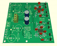
I made a couple final tweaks to the silkscreen to make assembly easier for the beginner. Attached are screen shots of the layout as well as a couple of 3D views of the board, one fully populated and the other without the power supply section populated.
There are a couple of different ways to configure the board. You could only populate one half of the gain stage circuitry, yielding a 2-channel (stereo) gain stage using a single op-amp, with PS or without. You can also use two boards to make an 8-channel gain stage (or any number of gain stages that are a multiple of two).
For a compact 8-channel version, the builder could use two boards, back-to-back. One board could have the PS section populated, while the other gets its power via the DC connector. Instead of running the DC power connector wires around the board edge, wires could simply be soldered between boards with a single twist to reverse the position of the V+ and V- leads from one board to the other.
I think the layout is flexible and should provide good performance for audio using the OPA2134 op-amp.
I will post the design files shortly. These can be sent to a PCB manufacturer. Anyone is welcome to manufacture and build the board for their own use - only commercial use is prohibited. This is now released into the public domain. Have fun!
.
Attachments


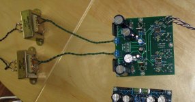
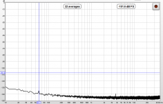
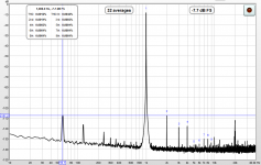
To provide an example of proof of concept, I built and tested an earlier version of this board that did not have a ground plane or the ground loop breaking resistors. I am attaching a picture of that (rev A) board and some quick measurements I took on the system using an LME49720.
The new board (rev C) should offer even higher performance than is shown in the attached plots.
.
The new board (rev C) should offer even higher performance than is shown in the attached plots.
.
Attachments

GERBER FILES AND BOM are found in that attachment
A zip file containing the GERBER FILES for the pcb and a spreadsheet containing a BILL OF MATERIALS with suggested parts (mostly from Mouser) is attached.
In the spreadsheet, at the top, enter the desired quantity for version A or B (with or without onboard PS) to get an estimated total parts cost assuming you have to purchase everything and do not have existing stock or other sources for the parts. Significant savings can be had if transformers or other expensive parts are already on hand. Please read the NOTES section at the bottom.
I want to make clear that I believe that this design works 100% but has not been tested and no warranty is expressed or implied. By using this design you assume all risk and agree that I, Charlie Laub, will not be held liable for any damages. This is for entertainment purposes only.
With that said, this should be a great gain stage for the miniDSP, a stereo preamp, or other audio project.
-Charlie
.
Attachments
Well, I ordered 10 boards. If you would like one, please message me. $13, shipped.
Please post your thoughts about the board, how you used it (what did you need the extra gain for?) and how it worked (or not) for your needs.
Note that you are free to choose the amount of gain used (the min gain is 1 for the non-inverting amplifier configuration). I think that if you follow the BOM you will end up with 12dB of gain (4x voltage gain). The more the gain, the more the noise floor is boosted up as well. Keep this in mind and use the minimum necessary.
Last edited:
I'd like to order some boards from a PCB manufacturer. Can someone give me advice on how to spec them? number of layers, board thickness, material etc? I've never ordered PCBs before.
thanks 🙂
thanks 🙂
I'd like to order some boards from a PCB manufacturer. Can someone give me advice on how to spec them?
number of layers, board thickness, material etc? I've never ordered PCBs before.
For small quantities usually you have to get 1oz copper, 1/16" thick pcb, 2 or 4 layers, G10 or FR4 material.
Often you have to order more than one pcb at a time, 3 or 4 perhaps. I'd recommend Osh Park or
Advanced Circuits for someone in the USA. A group buy might work out best.
http://docs.oshpark.com/services/
http://www.4pcb.com/33-each-pcbs/index.html
Last edited:
For small quantities usually you have to get 1oz copper, 1/16" thick pcb, 2 or 4 layers, G10 or FR4 material.
Often you have to order more than one pcb at a time, 3 or 4 perhaps. I'd recommend Osh Park or
Advanced Circuits for someone in the USA. A group buy might work out best.
OSH Park Docs ~ Fabrication Services
Full Spec 2-Layer PCBs - $33 Each | Advanced Circuits
Thanks Rayma. How do I know how many layers the PCB should be for this project?
- Status
- Not open for further replies.
- Home
- Source & Line
- Analog Line Level
- 4-channel gain stage with power supply