by
http://www.net-audio.co.uk/quad303upgrade.html
and
http://www.diyaudio.com/forums/soli...upgrade-output-stage-fully-complementary.html
are to find the suited steps for upgrading the output stage from quasi complementary to a true (fully) complementary version.
I want now to realize the opposite path - then I need only one kind of BjT/MOSFET power devices for repair service.
Before I can do this, I want to know exactly basically design rules. In case of triplets this is too complex for me for the safe avoidance of unwanted RF oscillations.
But in case of darlingtons it is already much clearer for me, because there is a normal darlington in one half and a Sziklai darlington (CFP-topology) in the second half in use - have a look in the attached PDF.
The main question are the resistor values in the emmitter - (R20) and collector line (R21) from the first stage of the Sziklai-Darlington, mostly allocated in the lower half.
The effect of the parallel mode elements (diode D3, capacitor C10) are clearly mentioned in various papers and the books, mentioned by
http://www.diyaudio.com/forums/soli...io-amplifier-books-overview-google-books.html
so as the threads like follow:
http://www.diyaudio.com/forums/solid-state/162310-how-identify-quasi-complementary-amplifier.html
http://www.diyaudio.com/forums/solid-state/88258-brother-quasi.html
http://www.diyaudio.com/forums/solid-state/53264-another-quasi-complementary-design.html
http://www.diyaudio.com/forums/pass-labs/6810-quasi-complementary-output.html
http://www.diyaudio.com/forums/solid-state/167394-quasi-amplifier-begginers.html
http://www.diyaudio.com/forums/pass...omplementary-mosfet-citation-12-taa-book.html
but not the ratio between the mentioned resistors.
This I want to know exactly.
Attachments
You can look in to Amslab (C200 amp) where various output schemes for the same amp is shown.
http://ampslab.com/projects.htm
That may give you some idea.
regards,
mandu
http://ampslab.com/projects.htm
That may give you some idea.
regards,
mandu
Thank you. Unfortunately I find only true-complementary output stages.You can look in to Amslab (C200 amp) where various output schemes for the same amp is shown.
http://ampslab.com/projects.htm
That may give you some idea.
regards,
mandu
Have a look at this thread:by
http://www.net-audio.co.uk/quad303upgrade.html
and
http://www.diyaudio.com/forums/soli...upgrade-output-stage-fully-complementary.html
are to find the suited steps for upgrading the output stage from quasi complementary to a true (fully) complementary version.
I want now to realize the opposite path - then I need only one kind of BjT/MOSFET power devices for repair service.
Before I can do this, I want to know exactly basically design rules.
http://www.diyaudio.com/forums/soli...complementary-50-watts-amp-4.html#post2728462
A good advice. Thank you very much.Have a look at this thread:
http://www.diyaudio.com/forums/soli...complementary-50-watts-amp-4.html#post2728462
Just completed on Gamut M250I (monoblock) 25 Kgs per channel.
An externally hosted image should be here but it was not working when we last tested it.
As I know, this brand don't use a quasi complementary output stage. Even if there are two identical output power N-CH MOSFET's.Just completed on Gamut M250I (monoblock) 25 Kgs per channel.
Each mosfet has its own push pull full complementary driver section. The driver section itself looks like a small wattage power amp. Have a look to
http://www.diyaudio.com/forums/soli...h-pull-pull-like-gamnut-whats-right-name.html
post #58 and post #59 mentioned the resistor R19 (in the schema from = R),Have a look at this thread:
http://www.diyaudio.com/forums/soli...complementary-50-watts-amp-4.html#post2728462
but without an ecaxtly investigation of the influence - like to see by comparing the graphs for the crossover region BjT MJ802/4502 vs. FET 2SK135/2SJ50 in the electronics world, MAY 95, page 388 and about the URLs
http://books.google.de/books?id=XT1...nepage&q="crossover region" Amplifier&f=false
and
http://www.bgaudioclub.org/uploads/docs/Audio_Power_Amplifier_Design_Handbook_4th_Edition.pdf
Last edited:
post #58 and post #59 mentioned the resistor R19 (in the schema from = R),
but without an ecaxtly investigation of the influence - like to see by comparing the graphs for the crossover region BjT MJ802/4502 vs. FET 2SK135/2SJ50 in the electronics world, MAY 95, page 388 and about the URLs
Audio Power Amplifier Design Handbook - Douglas Self - Google Books
and
http://www.bgaudioclub.org/uploads/docs/Audio_Power_Amplifier_Design_Handbook_4th_Edition.pdf
The first line is incomplete. It should read:
post #58 and post #59 mentioned the resistor R19 (in the schema from post #57)
The associated resistors in the circuit by fig. 4 and fig. 9 about
http://www.updatemydynaco.com/HistoricDocuments/GEAmplifier.pdf
are R8, R9 and R10. Have a look to this values.
http://www.updatemydynaco.com/HistoricDocuments/GEAmplifier.pdf
are R8, R9 and R10. Have a look to this values.
common design rules in general I don't find until now (have check various books and papers concerning quad 303 quasi triplets).
Read again post #1 for detail questions regarded this.
Most important issue by the use of quasi complementary triplets are suddenly occurred unwanted RF oscillations.
Because there are many different essembles for quasi triplets for the upper and lower half lies the problem in the nature of things.
Amazing for me is the stable operating of Quad's 303. This means, the correct design rules know at least the developer of this approach.
Last edited:
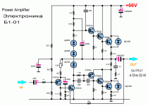
Hi Tiefbass !
Here is example of using output tripple inside of SSSR vintage Elektronika B1-01 integrated Amp.
Maybe this schematic can help you to get some answer to solve stability of quasycompl tripple .
Best Regards !
Thank you for this schematic. But I don't understand follow features:
1) Why a short to GND at the speaker output befor output capacitor (GND symbol at right hand of 6K8 DC-NFB resistor
2) Why 51Ω as serial resistance for the three serial bias diodes?
3) Why not Vbe multiplier (Transistor and one resistor and one variable resistor)
4) Why different kinds of resistors for the DC-NFB pad (maybe one with and one without unwanted parasitic inductivity)?
5) What is the benefit for this kind of compensation
Last edited:
Thank you for this schematic. But I don't understand follow features:
1) Why a short to GND at the speaker output befor output capacitor (GND symbol at right hand of 6K8 DC-NFB resistor
2) Why 51Ω as serial resistance for the three serial bias diodes?
3) Why not Vbe multiplier (Transistor and one resistor and one variable resistor)
4) Why different kinds of resistors for the DC-NFB pad (maybe one with and one without unwanted parasitic inductivity)?
5) What is the benefit for this kind of compensation
Thiefbass
1) There is no any ground sign there , since 6k8 resistor is actuallu 6k8 trim-pot .
2) If you look close you can see that 51R resistor have * marking beside them ( same as for 62K* res. ) , which mean that resistor is precise chossen to establish desired OPS quiescent current , basically we can replace fixed 51R res. with 100R trim.pot , and 62K res. with 100K trim.pot .
3) I think three series bias diodes is suficient to get relative stable bias for this simple Amp .
4) I don`t know
5) I don`t know
Best Regards !
thank you for clarifying.
check out also post #22 under
http://www.diyaudio.com/forums/solid-state/165165-edwin-20-watt-elektor-1970-may-3.html
and
http://www.diyaudio.com/forums/solid-state/174218-rebirth-phoenix.html#post2313409
An off-topic advice for you:
a good friend of me from your country has good contacts for speaker repair - go to
http://www.diyaudio.com/forums/mult...-chassis-transducer-altec-tannoy-jbl-etc.html
Please note:
My name is Andreas
My website is tiefbassuebertragung.de
Last edited:
- Status
- Not open for further replies.
- Home
- Amplifiers
- Solid State
- Design Rules for a Push-Pull Quasi-Complementary output stage