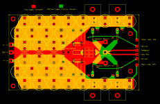
What do you think of the output board layout, grounding and current loops with the attached OPS PCB design?
I used to do it in a "standard" way of making a star ground at a point about 8cm away from the power supply common. All ground points, including the power supply common, speaker return, zobel, signal ground and a single connection point in the chassis were connected into this star point with wires.
Now when I think of it, while there was no hum or noise from that "standard" implementation, the current loops were larger than necessary.
The attached is my new design to minimize the high current loops. Using the power plane underneath the PCB to supply current to the output devices with a ground plane on the top side of the PCB, inductance and resistance should have been minimized. This ground plane is the supply common, though I mark one point and name it "PSU common" to be connected to the signal ground and chassis.
Speaker returns will be connected to either (1) or (2).
So basically, I ditch the concept of star point and put all of the high current points into a single PCB including the following (1) power supply reservoir capacitors; (2) Output Devices; (3) Zobel and Output Inductor / Resistor; (4) Speaker current return - the speaker outgoing wire and return wire will be in twisted pairs. A wire will be connected from the point marked as "PSU common" to the low current ground for IPS and VAS, as well as the chassis.
Obviously, IPS and VAS are housed in a separate board placed next to the OPS board.
Do you see any problems? I do hope that the inductor won't inject noise into the signal lines from the drivers.
Regards,
Bill
Attachments
Last edited:
The feedback trace is placed correctly, but feedback ground also needs to be directly to the load ground, to have a legitimate reference. If you put speaker return to the right of the output connector, then you'll have a clean ground trace to go next to the feedback trace. I see no problem with moving the feedback/Vout traces to the other side and circling ground around the output connector. You minimize current loops in the output stage, but without a ground connection going to the frontend along with the supply wires, you lengthen the current loops of the drivers.
You can visualize the driver current loops going from +Driver to +Rail. To eliminate trace gate inductance, you can extend the ground plane to cover the +Rail and +Driver traces, and then where those traces stop at connectors, connect the ground traces together to make a loop. Alternatively, you could run the Rail and Driver traces next to each other, both covered by the same ground "finger" so they are isolated by the ground plane but close enough to minimize stray inductance.
So my idea is, if this can be done, is to run the gate and rail traces next to each other under the FET source resistors. From the large film caps, extend ground fingers going under the rail/gate trace pair and ending at the edge connectors. This way the rail and gate traces don't interfere, but the current loops get to choose the path of least inductance. This way the Rail traces can also be taken from the power plane closer to the large array of caps and not so close to the FETs.
Wide traces minimize inductance, but when you have a ground plane inductance is pretty controlled, so you only need the trace to be big enough to carry your maximum current. I may be wrong on this. If the frontend takes say 25mA, the traces probably don't need to be very large.
Again, I'm not a PCB expert, so I may be terribly wrong, and hopefully someone will correct me. If you just add a ground reference to the edge connectors, it will still be no worse than the majority of boards I've seen (not too many), and probably better because of the highly effective power layout.
The feedback trace is placed correctly, but feedback ground also needs to be directly to the load ground, to have a legitimate reference. If you put speaker return to the right of the output connector, then you'll have a clean ground trace to go next to the feedback trace. I see no problem with moving the feedback/Vout traces to the other side and circling ground around the output connector. You minimize current loops in the output stage, but without a ground connection going to the frontend along with the supply wires, you lengthen the current loops of the drivers.
Thanks, Keantoken.
I think I have caused a bit of confusion as I have not made it clear in the PCB image. The edge connectors on the right edge of the PCB are to be connected to the low current IPS and VAS board only, and not to be connected to the speaker wires.
A 2uH air core inductor (and a 8R resistor) will be mounted vertically to the PCB at the exact point marked "Output L/R", possibly with 3cm lead, to route this high current path away from the IPS and VAS board. This is not shown in the PCB. The speaker return wire will go with this outgoing wire after the inductor in twisted pair. I think in this case the current loop as well as inductance are at the minimum.
You can visualize the driver current loops going from +Driver to +Rail. To eliminate trace gate inductance, you can extend the ground plane to cover the +Rail and +Driver traces, and then where those traces stop at connectors, connect the ground traces together to make a loop. Alternatively, you could run the Rail and Driver traces next to each other, both covered by the same ground "finger" so they are isolated by the ground plane but close enough to minimize stray inductance..
That sounds a good idea. Indeed, I have had the same idea just (1) have not had the time to do it yet; (2) am a bit worried about the dirty ground in at the OPS being too close to the IPS+VAS ground, but should be no big deal; (3) a bit worried about the increased capacitance for the driver track. I will find some time in the next two hours to implement this idea and post a new picture.
Extending the ground plane to cover the driver track and the output track will add some pF to the tracks (to ground), but I guess that does not really matter as it may be good to shunt some very high frequency to ground anyway at the input and output of the output device. Right or wrong?
It will add some capacitance, but it will be no larger AFAIK than the capacitance of the FETs themselves, and due to the ground plane the capacitance will be much less likely to interact with stray inductances.
I know that the edge connectors go to the frontend. But why is there no ground connection to the PCB as well? Speaker return needs to be connected to frontend ground, with the shortest trace possible. As it is, you will need to run a wire from PSU common to the frontend board, which could be made redundant and less parasitic by including the ground connection at the edge.
If you want to keep the L/R from radiating, why not put the L somewhere away in the case, using a twisted pair, and keeping the R at the board? This way you can put the L anywhere you want.
But why is there no ground connection to the PCB as well? Speaker return needs to be connected to frontend ground, with the shortest trace possible. As it is, you will need to run a wire from PSU common to the frontend board, which could be made redundant and less parasitic by including the ground connection at the edge.
I separated different ground points in the IPS and VAS board. The rail decoupling ground may be the dirtiest and it will be connected to the ground point as you suggested. The TPC ground point will be connected to the same point as well via a separate track. The input ground and the feedback ground points are connected. I don't like the idea of using a 10R resistor to separate the input ground from the star ground, as subjectively this makes the sound worse. I am planning to use a long wire to connect this point to the "PSU common". Unfortunately, this most sensitive ground point (input and feedback) is at the other extreme edge of the IPS and VAS board so it has to be connected to the "PSU common" point via a wire. I really don't know if inductance in this wire matters or not. Other ground points can be routed to the edge close to the OPS board.
Speaker ground to be connected to the frontend ground? I think speaker ground is the dirtiest and we don't want it to contaminate the IPS and OPS ground. I think PSU common is the "reference" ground point therefore all ground points should be connected to this one. (Sorry, in other words, I still have the star ground concept, only to make the star right at the centre of the ground plane and make it up close to the output devices and speaker return).
If you want to keep the L/R from radiating, why not put the L somewhere away in the case, using a twisted pair, and keeping the R at the board? This way you can put the L anywhere you want.
I guess that the distance here to the sensitive wires is the same distance between the RCA input jack and the speaker terminals so perhaps it makes little difference.
A major reason to place the inductor close to the OPS board is that I want to minimize the capacitance between the output point and the inductor. I think the purpose of the inductor is to counter the reactive capacitance in the load, so perhaps we should not allow capacitance before the output inductor. Twisted pair would give quite a bit of capacitance. If twisted pair is not used then the loop is larger and magnetic interfereance may occur.
I have a question about the Zobel ground point.
Currents that can pass the Zobel must be of very high frequency well beyond the audio bandwidth. They must be irrelevant to the audio waves and must be dirt. Should we put the ground point to the chassis, instead of the PSU common?
I can think of this because I experimented puting the input shunt capacitor ground to the chassis instead of the input ground and the sound instantly became clearer. If you have not tried this you should try it.
kgrlee says that every input connector should be immediately decoupled to the chassis with a short capacitor, for RF measures. So the idea is to decouple RCA ground to chassis ground. This goes for speaker connectors and PSU connectors as well.
The problem is that the amp zobel may mitigate RF from interference, but it needs to be directly from output to decoupling ground for minimum inductance so that it performs it's function for the amplifier. So you would need to use two zobels, one at the PCB and another at the chassis.
Speaker return is no more dirty than Vout, unless you put reservoir return between amp ground and speaker return. And if it IS dirty, then we NEED to put amp ground there so the dirt isn't added to the output! Every node could be seen as dirty, it's where it is relative to amp ground that counts. You need to worry about making amp ground clean, rather than making speaker return clean and leaving amp ground dirty because then amp output will be dirty.
The connection between amp ground and power ground having significant inductance is a problem, because this inductance is a dramatic lengthening of the current loop between frontend and output. This current loop is shorted by the frontend decoupling of rail power to PCB ground, but the shorting occurs through a noisy path.
The ground side of the feedback network should be just as accessible as the Vout side, so why not extend a trace from here and run them together to the OPS board?
As for the L/R, the twisted pair may have some capacitance but this is bypassed by 8R at the PCB. The Fc of 8R and 50pF is much higher than anything we would normally worry about.
Thanks again, Keantoken.
Two more questions if you don't mind.
(1) I have had two zobels, one on the amplifier PSB and the other on the speaker terminals on the speaker side, not the amplifier side. If the speaker terminals on the amplifier side need to be RF terminated (that sounds like a plausible idea), how would you do it? I imagine one zobel (8R+56nF) from the speaker out to the immediate chassis point, and another small C (???) from the speaker return to the immediate chassis point. Since there are two zobels within the amplifier, would you reduce the capacitance of the Zobel C to half for each, such as 56nF?
As for RCA input RF termination, I would terminate the input signal via a 50R + 100pF or something, and a 10nF or something connecting the shield (ground) to the immediate chassis point.
(2) Earlier you mentioned to reduce the inductance of the driver track. Isn't a bit of inductance there good? I heard some implementation uses ferrite bread there to remove the high frequencies for better stability. Provided that the gate resistor is sodered directly on the gate, before the resistor the inductance does not appear to cause any harm. Even a long wire with 300nH in simulations does not cause any problem. I earlier thought that I could use long shielded cable as the driver wire (of course, shielded cable would have lower inductance) but I guess shielded cable may not be necessary.
Ferrite beads, at the frequencies in question, are lossy. They behave like L/R series to the gate. It's like shorting the gate stoppers with inductors so that the gate stoppers don't affect lower frequencies. With your current design, inductance may not be a problem. However if this OPS board is to potentially interface with multiple frontends, you will want minimize inductance to increase compatibility. Low-inductance gate traces would make this board compatible with faster frontends which means less treble distortion. To me this is a significant feature and takes the board to a higher level.
Also: Shortening current loops also means shortening antenna length. Decrease in trace inductance and current loop size means less parasitic and stray interactions, and less susceptibility to RFI.
A shielded cable for the driver is a neat idea, except that there is no equivalent return path for the gate current loop, which splits between the source and drain. You gate current loop then flows through the output zobel to ground, and through the rails. You would need to force the return current through the cable shield, and you would not be able to do this without mixing unwanted signals like rail noise. The PCB option is less tedious, and furthermore your ground plane can shield multiple traces - making it like a 2-conductor coax. This advantage allows you to shorten the gate current loop without pulling noise from the rails.
I agree with your suggestions on termination. I would not divide the output zobel, because the L/R has to go between. At the very least, the R in the zobel needs to be the same, and it may be okay to divide the capacitance between the amp and chassis zobels. But there is a risk that the amp will not like this. For least risk I would leave the zobel as is and add a new one at the chassis.
To my eyes it does not seem to follow Douglas Self's detailed advice on exactly where on a pcb to connect the feedback. The NFB take-off point needs to be >after< the output 'split,' not at the split...? (As on the cover illustration of Self's amplifier book)The feedback trace is placed correctly...
If the speaker return is taken on the feedback side of the board then it will be. Although I guess I would prefer a bit more trace in between to get further from the summing gradient? If we could calculate the parasitics here then we'd know for sure, which must be more valuable than guessing.
Last edited:
Although I guess I would prefer a bit more trace in between to get further from the summing gradient?
Keanetoken,
Sorry to invade the thread but what is this summing gradient?
Thank you.
At the summing point where the source currents combine, there is a voltage gradient across the copper area causes by copper resistance. You choose one spot as the feedback node and feedback ensures that all parasitics for that spot only are corrected. If you take speaker out from a different point along the gradient, you get distortion. Even inside the gradient tap point there may be a significant voltage gradient, so taking output from one side of the tap point may still result in distortion. Therefore you move the speaker output away from the summing point and closer to the feedback input along the feedback trace; the charge gradient quickly dissipates.
This is much more evident in reservoir grounding where the amps flowing are several times more than the speaker output. There may be a gradient across the star ground bolt if you put star ground right at the reservoir summing point, so even the direction the wire tab faces may cause ground noise. Better to put some thick wire between the gradient and the star ground.
This is much more evident in reservoir grounding where the amps flowing are several times more than the speaker output. There may be a gradient across the star ground bolt if you put star ground right at the reservoir summing point, so even the direction the wire tab faces may cause ground noise. Better to put some thick wire between the gradient and the star ground.
"The devil is in the detail" it seems. So if I understand this correctly you are describing a multi star point system where any nodes with large currents and hence gradients are spaced apart.
You really are a mine of useful information. 🙂
You really are a mine of useful information. 🙂
I've always thought that the advantage of a dual bridge PSU was that it had greater maximum power dissipation. And hence never bothered with it, as big bridges are relatively cheap.
To my eyes it does not seem to follow Douglas Self's detailed advice on exactly where on a pcb to connect the feedback. The NFB take-off point needs to be >after< the output 'split,' not at the split...? (As on the cover illustration of Self's amplifier book)
It doesn't violate Self's book. However that wire is pretty short in this case. I can extend that piece of wire to an extra 10mm-15mm on the PCB. The price to pay is that the high current speaker wire will get a bit closer to the VAS board.
I am now thinking about connecting the rails and ground from the VAS-IPS board to the earlier stage of power supply reservoir caps instead of taking short connection points to the OPS board.
I understand that this will make the current loop much longer. However, since I use a heavy duty passive filter DC-RC-RC-RC-RCCC for the VAS and IPS rails, I am afraid that the switching noise from Diode D gets too close to the output devices. I think I had better route it away from the OPS board so that the switching noise doesn't influence the output device and feedback as much.
What do you think?
Last edited:
- Status
- Not open for further replies.
- Home
- Amplifiers
- Solid State
- Grounding and Minimizing the Current Loops