Did I already mention that I´m going to build in a 3.5mm jack plug? So I´ll only have one ground for both channels...
Done - for the "real" tracks...
What would be if I would move the power-ground into the star-ground?
And is anyone able to tell me how often the copperwire has to be wound around the resistor for R/L? ANd does it have to have a diameter of 1mm? or would 0.8mm would work too?
What would be if I would move the power-ground into the star-ground?
And is anyone able to tell me how often the copperwire has to be wound around the resistor for R/L? ANd does it have to have a diameter of 1mm? or would 0.8mm would work too?
And is anyone able to tell me how often the copperwire has to be wound around the resistor for R/L? ANd does it have to have a diameter of 1mm? or would 0.8mm would work too?
I used 0.8mm, 10 turns tightly on the body of 10ohm/3W resistor.
Here's how I did the layout. Although the traces are only 86 mils in width, they are covered with around 0.5mm solder layer and thy withstanded an unwanted shortcircuit between the negative rail and ground. The chip leges melted, the tracks were fine.
Attachments
The inductance isnt critical. 0.8mm is fine. I actually used some enamelled wire from the +5V choke in an old PC PSU 🙂
Simply wind enough turns around the body of the 10 ohm resistor. This is plenty.
Simply wind enough turns around the body of the 10 ohm resistor. This is plenty.
And who wants to tell me wich inductivity i need? 😀
The datasheet. 10 Ohm and 0,7 µH.
No Edit-button again...
I winded a pair of aircoils now, 0.75mm wire and pretty exactly 0.7µH 🙂 Now I´ll just have to fit them into the PCB
I winded a pair of aircoils now, 0.75mm wire and pretty exactly 0.7µH 🙂 Now I´ll just have to fit them into the PCB
They do specify an inductance but in all truth, its really not that critical. If you have the means to measure inductance i'd be interested to find out what my suggestion of just winding the turns around the 2W resistor produces.
No sorry, at the moment I do not have the necessary measurement device...
But do you maybe wanna give ma an answer to my question about the "GND-pad"? 😀 So that I finally can finish my PCB 🙂
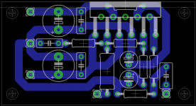
Edit: So now - this is it:
Everything ok now?
The two single vias are for the aircoil! I hope it won´t affect the amp, as though it´s pretty near?!
But do you maybe wanna give ma an answer to my question about the "GND-pad"? 😀 So that I finally can finish my PCB 🙂
Edit: So now - this is it:
An externally hosted image should be here but it was not working when we last tested it.
Everything ok now?
The two single vias are for the aircoil! I hope it won´t affect the amp, as though it´s pretty near?!
Last edited:
Rz top end must connect to the chipamp output. Disconnect that trace that goes down to the speaker +.
If you want to add an extra R+C after the L//R, then do that across the output terminals. This catches the back EMF and/or interference before it gets too far into the chassis/feedback loop.
Are you planning to add RF attenuation on the back of the PCB? You have omitted it on the front.
Your latest layout has returned to putting the feedback resistor across the chip pins and similarly the +ve supply to pin5.
Keep the separation of the decoupling Ground from the PCB star ground. This will facilitate a multi-channel amplifier. Use or remove that link you have shown.
You mean an extra R+C, altough there already is Rz and Cz?
And yes of course, Rf and the connection for Pin5 will be made on the chips pins 🙂
Edit: Now I´ve understood - >after< L//R 😀 So does this mean, that my Zobel-Network is senseless??
And yes of course, Rf and the connection for Pin5 will be made on the chips pins 🙂
An externally hosted image should be here but it was not working when we last tested it.
Edit: Now I´ve understood - >after< L//R 😀 So does this mean, that my Zobel-Network is senseless??
Last edited:
Hi,
most designers and builders use a Zobel (R+C) at the PCB output.
Many also add in L//C to create the Thiele Network of R+C & L//R.
A few and I am now a convert to this, use a Pi network, where an extra R+C are added to give R+C, L//R, R+C.
This still gives a nice load at both low and high frequencies but does a better job of attenuating back EMF and interference.
Good 🙂 Wich values do you recommend for R+C between the outputs? 2.7/100, too?
P.S. So... we´re finished now? Nothing more to correct in my layout? 🙂
P.S. So... we´re finished now? Nothing more to correct in my layout? 🙂
Last edited:
Oh and you told me that Rm = 22k will turn on my amp when the supply-voltage reaches 9V - what´s the meaning? Isn´t that ok?
The mute pin is there to allow the user/operator to use the mute to defeat start up noises or to silence the amp at will.
Connecting a permanent resistor as you have shown defeats the mute.
The amp will attempt to turn on as soon as the Low voltage threshold has been passed. That may generate unwanted noise at the output of the starting amplifier.
Connecting a permanent resistor as you have shown defeats the mute.
The amp will attempt to turn on as soon as the Low voltage threshold has been passed. That may generate unwanted noise at the output of the starting amplifier.
Good 🙂 Wich values do you recommend for R+C between the outputs? 2.7/100, too?
P.S. So... we´re finished now? Nothing more to correct in my layout? 🙂
for the Pi filter I reduce the two Cs to 47nF.
The first R ~1.5* speaker impedance.
//R ~ 0.5* speaker impedance.
Last R ~speaker impedance.
i.e. for 8ohm speaker
12r + 47nF
4r //1uF
8r + 47nF
At very high frequency when the L is effectively infinity and the Cs are short circuit; the load is ~6r.
At low frequency when the Cs are near infinity; the speaker sees 1uF in series with it's own impedance.
- Status
- Not open for further replies.
- Home
- Amplifiers
- Chip Amps
- LM3886 Layout ok?