Eva said:The huge pitfall of collector/drain output stages is the complete lack of quiescent current and cross-conduction control when large high frequency AC signals are amplified.
Can you elaborate on this? If the designer intended it to be a class AB push-pull output stage, then up to a certain amplitude, either the p or the n will not have current while the other provides all the current to the load.
rlim said:
Can you elaborate on this? If the designer intended it to be a class AB push-pull output stage, then up to a certain amplitude, either the p or the n will not have current while the other provides all the current to the load.
That's true only if you consider an output stage with ideal devices having infinite bandwidth and constant Vbe and Vgs turn-on thresolds, but it's not true at all for real transistors whose turn-on thresholds are dependent on Vce and Vds and which take a certain time to start and stop conducting. Also, output stage has to be intentionally slowed down with gate and base stopper resistors to get a stable amplifier, which further contributes to create current tails and unexpected cross-conduction. Simulation software WON'T predict these effects in most cases because transistor models are not that accurate.
Eva said:
That's true only if you consider an output stage with ideal devices having infinite bandwidth and constant Vbe and Vgs turn-on thresolds, but it's not true at all for real transistors whose turn-on thresholds are dependent on Vce and Vds and which take a certain time to start and stop conducting. Also, output stage has to be intentionally slowed down with gate and base stopper resistors to get a stable amplifier, which further contributes to create current tails and unexpected cross-conduction. Simulation software WON'T predict these effects in most cases because transistor models are not that accurate.
My my, somebody's been busy...
Veeeerry nice..
Toimal vbe..dey be da teekit..
Your tails... be they 100 usec level or 100 msec...ie, silicon thickness or case thickness.
Cheers, John
Eva,
The phenomenon that you're talking about.....does it occur with emitter/source follower outputs?
Thanks.
The phenomenon that you're talking about.....does it occur with emitter/source follower outputs?
Thanks.
rlim said:Eva,
The phenomenon that you're talking about.....does it occur with emitter/source follower outputs?
Thanks.
Try to measure current consumptions on different frequencies.
😎
Eva said:The huge pitfall of collector/drain output stages is the complete lack of quiescent current and cross-conduction control when large high frequency AC signals are amplified. Even popular circuits like SKA suffer very badly from that phenomena..
Hi Eva,
have you tested SKA, if not would you still say that SKA suffers from cross conduction?
Cheers Michael
Leolabs said:Why collector/drain output stages are so rare???
Is it because of stability issue???
.
First, common drain outputs are not so rare,
but not at all as common as common emitter.
And you are a bit right in 'stability guess'
- I think generally common drain can be a bit more instable
as well as They are Often VERY FAST amplifiers.
So when building such amp, you may need to do some things to stabilize.
But this goes for most all amplifiers - even the standard type.
--------------------------
Common collector output has got Voltage gain (usually considerably more than 1.0) in output stage.
And this gain is effected by the load.
While common emitter has got less than 1.0 ( something like x0.90-0.99 in a best case ).
This makes common emitter amplifiers a bit less sensitive to loads.
In my opinion.
---------------------------
We can not say, that common collector or common emitter is better.
They can do good, both.
For example in PreAmplifiers, without a buffer follower stage,
the feedback is taken directly from common collector output.
This is not unusual for low power Class A pre amplifiers.
I have a number of bookmarked links to Common Emitter ( Drain ) amplifiers.
They are a challenge and sure are very interesting to design, to build and explore.
lineup
Lineup,
now you are really mixing up some things here... 😀
Hint: Common drain -> Source follower -> certainly not so rare! 😉
Cheers Michael
now you are really mixing up some things here... 😀
Hint: Common drain -> Source follower -> certainly not so rare! 😉
Cheers Michael
Hi,
Some examples :
Bipolar collectors output :
Wim de Jager, Erik van der Ven, Ed van Tuyl, ELECTRONICS WORLD, December 1999 pp. 982 – 987
Mosfet drain output :
see the Transnova schematics at the Hafler site.
Some examples :
Bipolar collectors output :
Wim de Jager, Erik van der Ven, Ed van Tuyl, ELECTRONICS WORLD, December 1999 pp. 982 – 987
Mosfet drain output :
see the Transnova schematics at the Hafler site.
Ultima Thule said:Lineup,
now you are really mixing up some things here... 😀
Anybody that does not understand my post message - probably has hang up on single words and expression.
Messages, posts are made up by sentences.
Sentences are made up by words and expressions (combination of words and terms).
Words are made up with letters, characters of alphabet.
If I write:
- Helo, Ultima Thule.
the usual reply would be:
- Hello, Lineup.
Because this exchange of thoughts, messages is a context,
that shows the receiver got the message, the words
- even though was a detail in message not correct.
Some, often people with negative attitude, will try to look for the details
like bad spelling, bad improper words or terms.
Because they like to take away attention from message
or wont accept to take message.
Maybe they even have another view, that was proven not very good
and instead of accepting - they try to get out of Context .. out of Topic
by focus interest on side notes .. on details.
Details that are not so important
for those who understand the intentions and what the sender is saying.
this is not true communication - it is not good communication
But i can agree so much, that it is very good we use same terms for same things in amps
thanks for correcting my terminology
- i have no whatsoever Degree from Any School in Electronic Engineering.
In my plain world, something that is COMMON, share same thing
in my mind this is the output joint.
And when Collectors are joined together at one point
this is for me 'common collector'.
But this is for those using electronic terms and language
is not the same as my definition and I have to use some other expression.
So exchange all places where I say 'common collector' with
the topic starter 'collector/drain output'
and so you will be able to take part in discussion, Ultima Thule.
As you will know what I mean.
Hope everything is clear now.
No Regards
lineup
hi
Leolabs
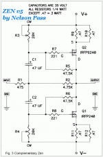
I post here one of my favourite Nelson Pass amplifier designs.
Zen version 5 - ZEN v5
It is a much too little recognized amplifier.
It is a remarkable way to setup a push-pull Drain-Output Stage, with negative feedback.
Without any drivers!
There are a couple of projects that is building this amplifier,
in Pass Labs forum.
Do not fool yourself .... is not as easy to setup a good build of Zen v5
Good Simplicity is difficult!
take a look!
Regards
lineup 😎 just loves the simplicity of ZEN V5
Leolabs
I post here one of my favourite Nelson Pass amplifier designs.
Zen version 5 - ZEN v5
It is a much too little recognized amplifier.
It is a remarkable way to setup a push-pull Drain-Output Stage, with negative feedback.
Without any drivers!
There are a couple of projects that is building this amplifier,
in Pass Labs forum.
Do not fool yourself .... is not as easy to setup a good build of Zen v5
Good Simplicity is difficult!
take a look!
Regards
lineup 😎 just loves the simplicity of ZEN V5
Attachments
More information on the above amp :
Wim de Jager, Erik van der Ven, Ed van Tuyl
ELECTRONICS WORLD December 1999 pp. 982 – 987
"This class-AB common-emitter power amplifier incorporates a new current-mode class-AB driver circuit to obtain good thermal stability of the quiescent current in the output stage. It also guarantees non-zero currents in the output transistor that is conducting the residual current, avoiding HF switching distortion. Maximum output voltage is near to the rail to rail limit. Saturation of the power transistors is avoided, resulting in fast recovering from clipping. The circuit has an excellent stability due to a phase margin of 85 ° with a b 1/34"
Interesting, so far people have pointed out a lot of well-known, and also some less well known, problems with common emitter/source outputs. But nobody so far has given a clue what the supposed advantages are, except from the obvious one that we get gain also in the output stage. (I am not counting Sziklay pairs here, since I think they are better thought of as a single compound component and thus correspond better to emitter/source followers, although having some differences).
I have vague memories of the text that accompanied the Maplin 50 W amplifier. It had two sets of output devices, driving the load in parallel. One claimed advantage for the amplifier was that it did not require matching of the output devices.
Presumably the common emitter configuration allowed for some local feedback to be applied (in the usual way) thus reducing the effect of hfe variations. I remember there being low value resistors between the supply rails and emitters, which would provide local feedback, and of course promote current sharing between the parallel OP transistors.
Sorry that I am unable to find a circuit diagram for the amp, it would aid explanations immensely...
Ed
ZEN V5 is a really funny circuit, it will amplify power supply ripple nearly as much as the input signal, and output stage bias current is not regulated and completely dependent on the magnitude of the supply rails instead. Such a circuit is only to be powered by attaching the PCB directly to the output binding posts of a high quality bench power supply 😉
Hi Lineup,
cheer up ol' buddy, it's soon christmas!
Hi Eva,
did you notice my post to you?
Cheers Michael
cheer up ol' buddy, it's soon christmas!
Hi Eva,
did you notice my post to you?
Cheers Michael
Christer said:I(I am not counting Sziklay pairs here, since I think they are better thought of as a single compound component and thus correspond better to emitter/source followers, although having some differences).
I agree but don't miss that a sziklay compound may be arranged to have some voltage gain if need (at expense of others performarce of course).
Ciao
Piercarlo
PS - Merry Xmas to all! 🙂
Ultima Thule said:
Hi Eva,
did you notice my post to you?
Cheers Michael
Yes, I noticed it, but I don't like to be always the one that does the dirty work to end up posting oscilloscope screen captures that nobody seems to understand anyway. If people assume that some circuit is free of flaws without taking the effort to test it, then I will leave them believing so.
Piercarlo said:I agree but don't miss that a sziklay compound may be arranged to have some voltage gain if need (at expense of others performarce of course).
I thought Sziklay pairs always had the input transistor emitter tied to the output of the pair (ie. what we would consider as emitter/source if treating the whole pair as a compound transistor), in which case we cannot get any voltage gain >1, as far as I can see. Is there any other variant that I don't know about? Or did you mean using the pair in "common emitter" configuration?
- Status
- Not open for further replies.
- Home
- Amplifiers
- Solid State
- Why collector/drain output stages are so rare???