Hello everyone!!!
I am writing to you from Italy, and finally after a long time, I am about to start the construction of my final audio system (at least for a while)!
I would like to present the project, and ask you as well as your opinions, some advice...
Ready, go!
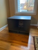
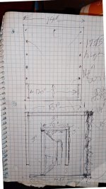
The room is 4,3x10mt big, the system will be placed on the narrowest wall.
At the end of the room there are stairs going down, so it is not enclosed. The roof is built with wooden beams placed crosswise, relative to the placement of the system.
The thermal insulation of the house was made cork, which could also help with the sound.
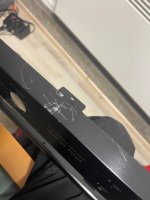
This Is the room:
I have always been fascinated by the sound of horn loaded systems, and after much thinking and many doubts, I am finally coming to a concrete final idea:
Three way, fully horn loaded, multi amplified system.
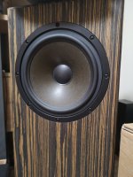
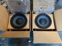
Bass with Radian 2216 neo driver, loaded in spiral box as designed by inlowsound:
https://inlowsound.weebly.com/spiral-bass-horn.html
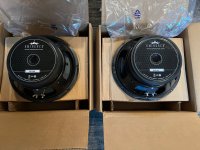
Double mid-bass with b&c 8pe21 driver, again based on inlow design:
https://inlowsound.weebly.com/135-hz-mid-bass-horn.html
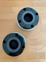
Mid-high with Radian 950pb driver, loaded on Arai 290 horn:
https://www.araihorn.com/p/arai-290.html?m=1
As a preamplifier I have my eye on a model from Black eyes audio, tube with integrated dac:
https://blackiceaudio.com/daccd-pla...p_mzEsxKOnnsQ6TQI1Z-rqfXn0mVFk4z7O3LGaK6aC_vI
For the crossover I like the dbmark series:
https://dbmark.co.uk/products.php?i=XCAX
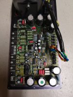
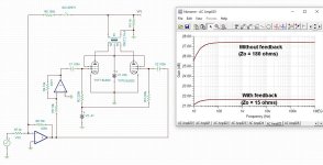
For the power amps I wanted to install class d amps made by IcePower, models and power ratings to be determined.
Indicative cutoff frequencies 130Hz/600Hz...
You will carry out the construction by me, and calibration together with a friend....
I am looking for a very dynamic and very exciting sound, but one that does not fatigue the ear....
I would like the frequency response to be as even as possible throughout the room....
I would like to have great quality both very low and at very high volumes...
Here is a picture of the possible arrangement...
Let's move on to the questions:
My first idea was to make a four way system, and supplement the Radian driver with a tweeter higher up...
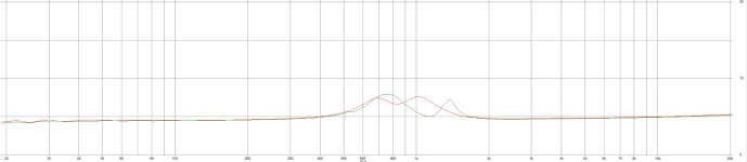
Given the problem of the distance of the emission centers, I decided to let the Radian driver do all the work up to 20KHz, but I have no idea how it will behave on the higher frequencies, like above 12Khz...
The changes introduced by Arai on its horn, compared to the Tad one, should give me a good off-axis frequency response even for the higher frequencies...
Has anyone had a chance to test this aspect of this driver? How do you think it will perform combined with this horn?
Also regarding the Radian driver, is the 8ohm version or the 16ohm version preferable?
Also the issue of dual mid-bass is to be able to have the most consistent frequency response possible across the width of the room, and so I should match 2+2 horns...
The designer told me that this horn has great punch and matches the bass very well, and that's exactly what I'm looking for....
The problem is the off-axis response, and I was thinking of solving it by doubling the horns....
How would you amplify the horns? Drivers in series?
Given the stability of the 4ohm amps, also parallel drivers?
Or even better, get the crossover with 4 outputs and put in two power amps?
I'm also a bit worried about tube preamplification....
Let's say I would like to give some warmth to the sound with preamplification, but then I would like to have the sharpness and control of a class d on the power amps...
I wonder how much sense this would make?
My friend who will help me with the calibration claims that we can use the crossover to create the kind of sound I want....
If this is feasible, I could easily opt for another non-valve preamplifier....
What do you think?
All opinions are welcome, thank you all very much, and Sorry for the english