There is a miner bug in this design when using the on board clock.
There is a little "click" sound when SM5842 reset the data input due to sync issue between on board clock and 8414 generated clock. I can think of few ways to eleminate the bug.
1. Use TCXO like NP but the cost to get a TCXO is not cheap.
2. Feedback the on board clock back to the cd player to cd player clock has to be in slave with the on board clock. This requires a modification of cd player and choose one player that can use 11.2896MHz clock.
3. Select another receiver IC that will accpet a external clock of 11.2896MHz.
Any body has any suggestion?
Anyway, without using the on board clock, the DAC itself can player very good sound and music to me.
I received a few enquiry about buying my D1 clone pcb and I am considering to sell it if the demand is more than 10 pcs. The price My offering will be US$25 per board plus $8 postage fee by registered airmail. Those interested please note down your name.
The board that I am going to sell will be the revision 2 which has the following changes:
1. Add a clock output socket pad.
2. Allow more space for all TO-220 heatsinks.
3. Add one more relay to select digital input.
4. Short circuit the Iout to BPO and thus no more jumper is required.
5. Enlarge some pad and connector hole sizes.
6. Add a ground connection for the ground plan on top.
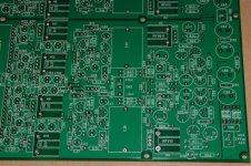
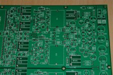
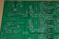
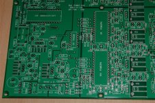
Board size is 8 x 10 inches, FR4 double size plate through board. Solder mask and silk screen printing on top side.
p/s: For those who has my ver 1 board, I will offer them at US$15 per board but the postage fee is still $8.
Regards,
Spencer
The board that I am going to sell will be the revision 2 which has the following changes:
1. Add a clock output socket pad.
2. Allow more space for all TO-220 heatsinks.
3. Add one more relay to select digital input.
4. Short circuit the Iout to BPO and thus no more jumper is required.
5. Enlarge some pad and connector hole sizes.
6. Add a ground connection for the ground plan on top.
Board size is 8 x 10 inches, FR4 double size plate through board. Solder mask and silk screen printing on top side.
p/s: For those who has my ver 1 board, I will offer them at US$15 per board but the postage fee is still $8.
Regards,
Spencer
More improvement:
7. Jumper to select the clock supply or 5842 supply for the 8414 IC. Clock regulator is not used in ver 1.
8. Use LM317T and LM337T regulators for all DACs.
9. Split the ground plan in sections: 8414, 5842, Input relay and logic IC, DAC left and DAC right.
10. Relocate the retification section (diodes and caps) of the 30V suply so that the last few filter caps will be close to a centre ground point.
11. Looking at input digital i/p section to see if relay can be eliminated or find a better way to reduce jitter introduction. This can be a daughter board put on top of the digital input section as it will take a longer time to develope.
Thanks for some of the feedback and the pcb count is now up to 5 persons.
Regards,
Spencer
I received feedback that other members are not able to post reply in this thread. Not sure if it is still the case now?
I received more than 10 enquiry about the ver2 board and I will build about 20 pcs to offer to those interested. It will take 2-3 weeks time. Update will be posted here when ready.
Thanks for the interest.
Spencer
I received more than 10 enquiry about the ver2 board and I will build about 20 pcs to offer to those interested. It will take 2-3 weeks time. Update will be posted here when ready.
Thanks for the interest.
Spencer
Hi,
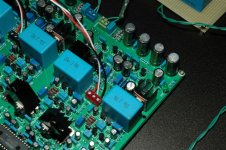
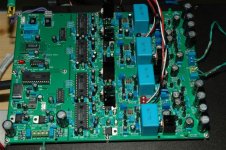
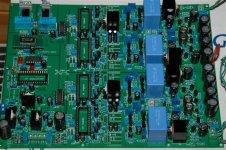
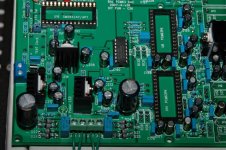
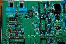
Changes on ver2 board has been freezed and design has released to pcb manufacturer today. Here are the changes:
Marking on board:
BAL PCM63 DAC
2007-4-v30
DIY Fun - CSK
1. Add a clock output socket pad (J20). This is reserve for the clock to feedback back to CD transport.
2. Allow more space and add holes for all TO-220 heat sink (total 15 T0-220 parts).
3. Add one more relay to select digital input (K2). Use jumper to select either XLR or RCA input (J8).
4. Short circuit the PCM63 Iout to BPO and thus no more jumper is required (J1-4 do not need anymore).
5. Enlarge all hole/pad sizes.
6. Add a ground connection for the ground plan on top near main filter capacitors (J19).
7. Jumper to select the “clock regulator” or “5842 regulator” for the 8414 IC (J17). Thue the regulator for 8414 will be isolated from 5842 when the on board clock is not used.
8. Use LM317T and LM337T regulators (better noise performance) for all DAC chips.
9. Add de-emphasis LED indicator (D32).
10. Split the ground plan in sections: 8414, 5842, Input relay and logic IC, DAC left and DAC right.
11. Relocate the rectification section (diodes and caps) of the 30V supply so that the last few filter caps will be closed to a centre ground point J19.
12. Add “+” mark for all E-capacitors for polarity identification.
13. Add resistor and VR for all PCM63 to trim the MSB (this adjustment is optional and reserve for diyer to play around the trimming of MSB).
14. Add Trimmer pot (R8, 9, 17 & 18) to adjust Jfet IV output level to match “+” and “-“ cycle. This is also optional and need accurate voltmeter and test CD. Do not solder the parts if diyer decided not to trim the output.
Spencer
- Home
- Vendor's Bazaar
- NP D1 DAC clone with enhancement