What about EML 20B as driver tube? It's got the specs we need.
I've considered it but then we are using a one-off expensive tube, a good match for an expensive IT coupled 2a3 build would be the EML 30A, does anyone have a spice model of the EML tubes? What I am seeing with spice is still no matter what you do a 2A3 output has less distortion with 1 watt output than a 4p1l. The issue is of course cost and the whole amp would depend on EML staying in business. Would hate to sink that kind of money into a tube that I can't replace in 2 years when I break it.
What is wrong with a simple input step-up transformer for the 4p1l dc coupled 4p1l? I emailed cinemag, they have a couple worth trying as does lundahl. Especially now days where most decent DAC's have a balanced output, might as well put the power to use. I guess I wouldn't build/or want a DAC that can't drive a small input transformer.
Just checked it out and it doesn't seem to have an advantage over 4P1L. And then... the price 
Here's a model I traced out with curvecaptor from the website curves. You can add capacitance yourself.
.subckt eml20b P G K
Bp P K I=((0.01153199547m)+(1.268936842e-005m)*V(G,K))*uramp((18.93571413)*V(G,K)+V(P,K)+(-48.94504672))**1.5 * V(P,K)/(V(P,K)+(-6.950280008))
.ends eml20b
Here's a model I traced out with curvecaptor from the website curves. You can add capacitance yourself.
.subckt eml20b P G K
Bp P K I=((0.01153199547m)+(1.268936842e-005m)*V(G,K))*uramp((18.93571413)*V(G,K)+V(P,K)+(-48.94504672))**1.5 * V(P,K)/(V(P,K)+(-6.950280008))
.ends eml20b
I've considered it but then we are using a one-off expensive tube, a good match for an expensive IT coupled 2a3 build would be the EML 30A, does anyone have a spice model of the EML tubes?
It is expensive and big! Bigger than the classic 2A3.
A real amp might be different. You have to select 2A3's to get low distortion at low level. I have (and have had during the years) nearly every kind of 2A3 and distortion at low level was one thing I didn't like. Best cases were 0.2% at 0.1W rising to 0.5% at 1W, average was 0.5% minimum and 0.7-0.8% for 1W......it was just irreducible unless employing some harmonic cancellatation being basically H2.What I am seeing with spice is still no matter what you do a 2A3 output has less distortion with 1 watt output than a 4p1l.
It's the drive. You have to have a really good preamp or DAC driver. It is possible but not given.What is wrong with a simple input step-up transformer for the 4p1l dc coupled 4p1l?
Seems to me it's a classic transimpedance amplifier.
<snip>... I was just pointing out that it's not a two stage amplifier, rather it has three stages, the first two being formed by two DC coupled active devices: a tube and a bjt.
The shunt cascode is not a 2-stage amplifier. Rather, it is a compound-device single stage amplifier.
Here are the checkpoints for its single-stage properties:
1. Signal voltage Nodes.
Number of signal input voltage nodes: 1
Number of signal output voltage nodes: 1
ALL other nodes in the circuit are at a dc voltage.
2. Signal Current Paths.
Number of signal current paths: 1
All other circuit paths carry only dc current. (I ignore grid leakage)
**
One does not count active devices and call this the number of stages - any more than a CCS-loaded stage should be called 2-stage.
The consideration of the number of signal Nodes and current paths is not a minor influence on the performance of an amplifier.
Every signal node is an opportunity for corruption by noise, and multiplication of distortion products.
For example, consider a voltage amplifier made from 2 triode stages. Any noise reaching the first stage from the power supply will result in multiplication of the signal frequencies and the noise frequencies. This action is identical to the operation of an AM transmitter - and leads to spectrum of sum-and-difference products in the output (Fsig + Fnoise) and (Fsig - Fnoise).
Now, this signal with cross-multiplied spectral products is fed to the input of the next stage, which multiplies them again! This is in addition to the corruption added by the 2nd stage on its own account.
The end result is a very wide smearing of spectrum in the output
I mention this to emphasise:
- why power supply noise sounds so very bad in a triode amplifier;
- why a 3-stage power amplifier sounds confused and cloudy compared to a (properly implemented) 2-stage design.
I also emphasise the advantage of the shunt cascode: it is possible to make a single-stage with a gain of 300, at very low distortion. At the same time the power supply noise is not only rejected by the CCS, but then crushed by the low-impedance action of the PNP emitter. The overall PS rejection is tens of dB better than an ordinary stage, even with CCS.
Even if you use shunt regulation, to control power supply noise, you are not safe.
A 2-stage amplifier multiplies distortion products: so the 3rd harmonics generated by the first stage are multiplied by the second stage to produce higher-order distortion.
These practical advantages make the shunt cascode even better than the simulations, because the real-world of noisy supplies, and EMI and nonlinear triodes are ever-present.
And here is set of 4P1L curves: compare constant current load (horizontal load line) versus load on emitter (vertical load line) and see the difference:
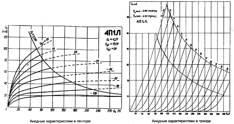
We can read very little from this drawing!
Anatoliy, please remember that this amplifier develops full power for a grid swing of only 400mV. To achieve the equivalent output with horizontal load-line, we must deliver more like 2V peak to the grid - in many cases, we will need an extra stage.
The Klausmobile measurements of actual valves gives a more accurate picture.
His curves do not reach 240V, that we require, but the performance of a vertical load line, for +/- 500mV show perfectly clearly that there are no reasons to suspect distortion.
http://www.klausmobile.narod.ru/testerfiles/4p1l.htm
Please see 2nd image (triode curves).
For instance, try operating point: Va=150V; Vg1=-6,5V Ia ~37mA
If you magnify the image, then carefully examine the vertical sweep for +/- 500mV of grid voltage, you will see equal spacing, even if measured with a vernier caliper, as I did.
The measurement actually looks better spaced for grid-swing 500mV vertical than it does for 2200mV horizontal (ie swings to get the same output).
And that is before we consider the fact that the shunt-cascode develops the output across a grounded resistor, has much better power supply rejection, greater gain flexibility - in this application, it allows lower number of stages.
Regal I'm with you , the cs4398 is one that like iron and is used for DSD recording by Korg,he just put out a dac/headphone.....
A 4p1L-4P1l with a little stepup transformer from cinemag, jensen, or lundhil should be drivable by any modern DAC, especially balanced DAC we should get an overal sensitivity of .5V.
Rod I like your approach (ruthless attempt to keep this a 2 stager), honetly yours isn't that much radicallly different than a CCS was 5 years ago. But when I look at your shunt cicuit I look at the vertical load line swinging current (not the 500 mV) you are mentioning.) I guess I agree with you fully that we don't want a three stage amp or a preamp, we would be better off using a damn 6n6p/5687/ecc99 driver than making it three stages.
But I need to try to simulate your shunt circuit with the 4p1l-4p1l, when it was firt brought up for 3a5-2A3 I tried it and it was just not stable, possibly my p-p wiring but I couldn't get a stable op on the bench and spice confirmed my finding.
A little steup transformer on the imput seems simpler and has the advantage with cmmr, eliminating the influence of cables, etc.
Cinemag just recommended this: http://cinemag.biz/output/CMOQ-2.pdf
1:2, if a DAC has an output impedance over 600 ohm its got issues and needs a preamp regardless.
1:2, if a DAC has an output impedance over 600 ohm its got issues and needs a preamp regardless.
The shunt cascode is not a 2-stage amplifier. Rather, it is a compound-device single stage amplifier.
The bjt which you call shunt cascode is a transimpedance amplifier receiving input signal via its emitter. The output of a transimpedance amplifier Vout = -Iin * R. In this case the resistor is 6k8. Do the calculation, it matches perfectly.
One does not count active devices and call this the number of stages - any more than a CCS-loaded stage should be called 2-stage.
There is no comparison between a CCS and the bjt transimpedance amplifier. The CCS only provides a load to the tube, in this circuit. What you call a shunt cascode is an amplifier in its own right. Please do the analysis carefully and you will see. Isolate the "shunt cascode," feed it from a variable current source, and see what it does.
Let's take a step back and look at this again. Rod, I'm not saying your solution is a bad idea. It might be an excellent solution and people could be extremely happy. I personally am exploring the idea to amplify the signal only with tubes, and in this thread, direct heated tubes. It's just a constraint I set for myself.
The bjt which you call shunt cascode is a transimpedance amplifier receiving input signal via its emitter. The output of a transimpedance amplifier Vout = -Iin * R. In this case the resistor is 6k8. Do the calculation, it matches perfectly.
There is no comparison between a CCS and the bjt transimpedance amplifier. The CCS only provides a load to the tube, in this circuit. What you call a shunt cascode is an amplifier in its own right. Please do the analysis carefully and you will see. Isolate the "shunt cascode," feed it from a variable current source, and see what it does.
Let's take a step back and look at this again. Rod, I'm not saying your solution is a bad idea. It might be an excellent solution and people could be extremely happy. I personally am exploring the idea to amplify the signal only with tubes, and in this thread, direct heated tubes. It's just a constraint I set for myself.
No, I do not call the BJT the shunt cascode. The shunt cascode is the whole stage: triode + PNP. They are are intimate unit.
what you suggest is that pulling the BJT out of my circuit allows you to make an amplifier with some of the qualities of the design I present. This may be so, but does not mean anything of consequence.
As the actual designer of the circuit, I have done the analysis properly. That's how it was developed!
Please look properly at Electrical Network theory, to see what constitutes a stage: it is the Nodes and current paths. With shunt cascode you only have one input, one output node, and one active current loop. This is the actual meaning of a stage.
We can demonstrate that the BJT is a support, not an active contributor to the transfer function like this:
The output is related to the input as -
Vout/Vin = gm.Rout
where gm is the effective transconductance of the triode, mA/V
This relationship holds for any signal, up to saturation of the stage.
Notice that only the triode and Rout are involved in the transfer function.
What this formula shows us is important: providing the base current error has been eliminated (I showed how to do that above) the BJT has no influence on the transfer function - if anything even less than a transistor in a CCS does.
Please model it yourself. Try doubling or halving the beta of the transistor, or its gm. In fact, you can make its gm 100 times higher, and nothing material will happen to the shunt cascode! You can swap the transistor for any other (that can handle the power), and nothing changes.
But if you change the triode for one that has one third the gm, the output drops by a factor of three.
So, our Shunt cascode performance is independent of the transistor - provided no gross parasitics are added.
If you don't think so, please present us with the analysis to show differently.
As Dave says, in a few years, making circuits of this kind will be as unremarkable as using CCSs, or transistor-followers is now.
For example, consider a voltage amplifier made from 2 triode stages. Any noise reaching the first stage from the power supply will result in multiplication of the signal frequencies and the noise frequencies. This action is identical to the operation of an AM transmitter - and leads to spectrum of sum-and-difference products in the output (Fsig + Fnoise) and (Fsig - Fnoise).
Now, this signal with cross-multiplied spectral products is fed to the input of the next stage, which multiplies them again! This is in addition to the corruption added by the 2nd stage on its own account.
The end result is a very wide smearing of spectrum in the output
I mention this to emphasise:
- why power supply noise sounds so very bad in a triode amplifier;
- why a 3-stage power amplifier sounds confused and cloudy compared to a (properly implemented) 2-stage design.
I also emphasise the advantage of the shunt cascode: it is possible to make a single-stage with a gain of 300, at very low distortion. At the same time the power supply noise is not only rejected by the CCS, but then crushed by the low-impedance action of the PNP emitter. The overall PS rejection is tens of dB better than an ordinary stage, even with CCS.
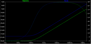
I agree that noise via the PSU is bad. I don't agree that the bjt you added helps in rejecting noise from the psu. In fact, when you posted this circuit a while ago, even without analysis, I mentioned my worry about the quality of the bias voltage for the bjt. Let's take them one at a time: there are two voltage sources, one coming from the supply above the DN2540, and one coming from the supply at the base of the 2N5401.
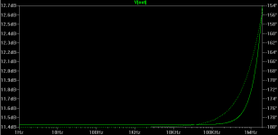
First, does the bjt crush noise from the PSU above the DN2540? We inject noise through V2 in the first picture. Look at the noise rejection if the bjt (shunt cascode) is not present, the green line V(dplate) being the output. The noise is decreased by about 88dB at 100Hz, which is about 40uV output noise for 1V PSU noise (disregarding any other sources of noise). The blue line, V(out), is the rejection of noise coming only through V2, in the simple circuit with both the tube and bjt present. At 100Hz, 76.6dB reduction in noise, or, in other words, 1V noise coming from V2 appears at the output as 148uV. I don't know how you observed tens of dB better rejection with the shunt cascode. What I see in this simple example is 11dB worse rejection of PSU noise.
Second, let's look what PSU noise rejection properties the circuit has if noise is coming only from the PSU at the base of the 2N5401 (bias voltage). In the last plot we see as that any noise coming thought this bias voltage is amplified by 11.4dB. It also does not cancel any noise coming from the PSU above the DN2540.
The conclusion is that the shunt cascode not only it makes line rejection worse, but it also amplifies noise coming from the bias voltage, so the bias voltage source better be EXTREMELY quiet.
These practical advantages make the shunt cascode even better than the simulations, because the real-world of noisy supplies, and EMI and nonlinear triodes are ever-present.
Except that the shunt cascode works against you in the real world of noisy supplies.
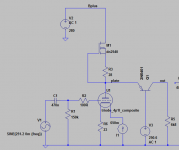
Attachments
All of this ignores simple practical measures, that will be found in the full circuit of this design.
In a competently built circuit, the PNP transistor will be a darlington, for reasons already explained above. In fact it will be a darlington made up of PBHV9040 x2 - since this excellent NXP transistor has constant Hfe for all reasonable currents - and a high value of 200 for Hfe.
The idle current in the circuit I presented is as much as 6mA. Therefore we must drive the darlington base with 250V at (6m/200)/200: ie in the region of 150-300nA, allowing for 2:1 variations in Hfe.
In other words regulating the cascode voltage - which is very necessary - is trivially easy to do.
My own circuits use a small number of SOT23 transistors (with a total BoM cost of a few pennies) arranged to give a stabilised shunt regulator. The noise level of this regulator models in the low microvolts - even for 1V of input supply noise. And the noise is unmeasurable with my present instrumentation.
Having easily established this level of regulation, we can look at the added noise rejection of the cascode PNP:
- the dynamic output impedance is 1/gm for a BJT. This is 1/(40 x Ic) - a fraction of an ohm in other words.
Now, we have a potential divider comprising of the CSS (high dynamic impedance) and the emitter of the PNP (very LOW dynamic impedance).
Compare this to the 1000 ohm anode impedance of the 4P1L.
All told, the idea of allowing a noisy reference into our circuit, when it only has to supply a fraction of a microamp - is needlessly poor design.
Relu, if you want to paint yourself into a corner, and exclude circuits that contain a single part you don't like - naturally that's your affair. But even if you don't like my circuit, surely you have better ways to spend time than mounting spurious attacks on mine? Why don't you design something better, and show it here, all fully worked out, and show how the problems can be solved. We still don't have a perfect solution for our headphone amplifier, even I will admit.
Rod, we are just discussing a circuit. I hope we are allowed to disagree and conduct a technical discussion. Please don't interpret it as any type of attack. This isn't about painting one in corners, not to me, at least.
I appreciate your contributions in general. At the same time, if you make some claim that I or someone else does not agree with, do you expect that we should just not express our different opinions?
I personally would be happy to be shown where I am in error.
I appreciate your contributions in general. At the same time, if you make some claim that I or someone else does not agree with, do you expect that we should just not express our different opinions?
I personally would be happy to be shown where I am in error.
Hi Relu,
Yes, it's just a circuit. Naturally, a proper scrutiny of circuits presented by designers is desirable..... but I think the attack on the power supply rejection was a bit too elaborate, given how easy it is to solve that problem.
It's more rewarding to put up original circuits here, if opportunities to develop them collaboratively arise - rather than only having to defend them.
And I do mean what I said about generating alternative schematics. We have 250+ posts in the thread, and about 2.5 full circuits, at the most. I think there's room for more ideas, more circuits, more solutions to the problem. Different builders need different power outputs, different impedances, and different gain. Some folks don't like magnetics, some don't like solid state - so one circuit is unlikely to fit all.
I would certainly enjoy to see more circuits on offer, that meet the brief - and even some that don't, if they have real merit.
I think it would be better for all, if the balance of effort swings more toward the Creative, rather than the Critical.
- Home
- Amplifiers
- Tubes / Valves
- The all DHT SET Headphone Amp