
Soon my hi fi will be totally home built except PU cartridge. One problem I want to solve is the preamp design. My only problem is switches. My old Quad 33 is always on death row and needs WD40 as recomended by Quad to clean them. It has an odd effect. Not great for about a week, then OK. When Dejan first replied to one of my scribles he mentioned the Armstorong 621. I have one as my radio ( 625 ). It is something of my brothers, so a very important part of my life. The gentleman who was Armstrong came to see me one day as my old boss was his friend.
Here is the diode switching of the Armstrong. So very simple, and yet it cures the Quad problems. The time constant of the so very simple circuit is to make it switch cleanly with a fading action. Would I be stupid not to try it ? Is not a forward biased diode linear ?
If I don't use it, it will be relays with earth braking. My PVR hums. It might only need a choke as it might be RF induced via SMPS. Even so to remove the input is best. To simplify I think I will fit a noise gate on a time delay. Diode switching looks interesting.
My OB speakers still have some nasties. Starting to love them. They show the world very differently and mostly better. I haven't yet topped $300. The shoutiness is mostly gone. When it is there often it is the microphone or EQ used. Radio 3 jazz made me jump out of my skin one night. It was the lady talking in the music. It was too real. It was like a ghost. Not bad for a PA driver and Chinese boom box 15 inch speaker used in socail clubs and the like. The Tweeter best of all at $12 a piece ( DT74/8 ). My ex as I said before was watching a film. She was very frightened and said " there are some very strange noises in the house ". She when shown the how and they why said. " It's impossible, the sounds comes from nowhere ". She even told me the food was very good. Why not when she was my wife ? We get on very well. Like she is my sister. That is correct as we don't hold back on saying what we think and don't really mind. I think she mostly left home because I don't dance and love my work more than.....? Sorry to say that could be true.
We're now squarely back to our initial dilemma. The key advantage of wide bandwidth low GNFB amps is in fact just that, phase shifts. With them, phase shifts are naturally lower, so the GNFB is left to clean up more mundane sorts of messes. I also consider to be important what is an amp's OPEN LOOP slew rate. It it's big enough to match the minimum required from an amp of that power, which is 1 V/uS/Peak Volt, then as far as I can see, there cannot be any higher order TIM/DIM artefacts and the phase shifts will be reduced before any NFB is required.
I just worked out that the final form amp I have just completed and is now ready for PCB design has an open loop bandiwidth of 120 kHz. Assuming that's so, and knowing the fact that it is rated at 100W/8 Ohms, which is 40 V peak, the open loop voltage slew rate works out at around 42 V/uS. Yet, according to my sim, classic THD at rated power is <0.03% into 4 Ohms and <0.02% into 8 Ohms. I'd like to be demonstrated how would that be audible under any circumstances.
And 1 will get you 10 that thing will sound more open, detailed and natural than far too many other amps.
And my proof is right next to me, in form of a Harman/Kardon PA 2400 power amp. It was built exactly along those lines, very wide bandwidth open loop response and very low global NFB factor of just 12 dB, yet it is capable of pushing around 40 Amps of current in short peaks into real world loads. It doesn't care what you connected to it as a speaker. Its slew rate is >150 V/uS, nominal power 170W/8 Ohms, but it was willing to fry two 4 ohm parallel lab resistors, each rated at 200W.
So, obviously, it is possible, and the results are excellent. Detail, space, "air" around the musicians, it's seemingly efortless and endless power resreves, do it, and I believe to this approach as well, credit.
Last edited:
No.Is not a forward biased diode linear ?

Not as bad as I thought. The last time I looked so closely at a diode curve was 1977. It was an EZ80. It might even sound nice ?
I think I can see a way to make it work that already suits my other ideas. As I dislike CD it would suit me to pot it down and make the prime sensetivity 100 mV to match my FM tuner. The pick up a Denon DL 110 needs about 40 dB ( 60 db 20 Hz ) gain to suit. I will pot the CD down lets say 3:1. The power amp might need 2.5 V rms. An OPA 2604 would be happy to do that. In the ideal world the amp will be 1 Vrms.
So how might we apply the 20dB test to other factors? An amplifier is more than THD and damping factor. IE how would you settle on a figure of merit for phase and gain margin?
One view is a function of negative feedback is to control and stabilize the gain and output impedance characteristics. Phase margin is the more common measure and an ideal figure would be 45 degrees.
Changes in phase start a decade below the -3dB frequency point of any simple RC network which will have a slope of 6 dB per octave. These characteristics typify what happens in a closed loop amplifier without compensation.
The trick is to calculate the frequency -3dB point. Let that be 1MHz for example. A well known direct approach is to use compensation around the main voltage stage to reduce the frequency response by a factor of 10 to 100kHz. The compensation should be such that the amplifier is stable at unity gain.
What is the part for Figure 10-200? I've never seen a simple diode curve become that constant-slope (i.e., resistive) before. The 1N4148 looks about right. Pease has some nice examples in the back of his book Troubleshooting Analog Circuits.
Not as bad as I thought. The last time I looked so closely at a diode curve was 1977. It was an EZ80. It might even sound nice ?
I think I can see a way to make it work that already suits my other ideas. As I dislike CD it would suit me to pot it down and make the prime sensetivity 100 mV to match my FM tuner. The pick up a Denon DL 110 needs about 40 dB ( 60 db 20 Hz ) gain to suit. I will pot the CD down lets say 3:1. The power amp might need 2.5 V rms. An OPA 2604 would be happy to do that. In the ideal world the amp will be 1 Vrms.
I also thought the same so went looking for real diodes. My interest is how far the curve can go before a simple switch is better. Hard to say. In RF the distortion is said to be third harmonic. This looks more likely to be second I guess? As I will be using an OP2604 there might be scope for looking at various currents. Will Google that book.
The EZ80 was that I had to set out the exam example for the other students. I was tasked with making sure the V/I diode experiment was working. Funny thing it was part of a higher level course! Seemed a bit easy to me. When I said I was told higher level seldom did practical stuff. We were training to be telecoms engineers. I transfered and did electrical engineering.
The EZ80 was that I had to set out the exam example for the other students. I was tasked with making sure the V/I diode experiment was working. Funny thing it was part of a higher level course! Seemed a bit easy to me. When I said I was told higher level seldom did practical stuff. We were training to be telecoms engineers. I transfered and did electrical engineering.
DVV you are right in that this subject is often side-stepped in the quest to eradicate distortion. We know the physics of what stability is, but how do we know our designs comply...in a good way?
I brought up the stability subject because of Nigel Pearson's 'factor of 10 goodness' and recent conjecture which is as follows:
We slave for hours on our simulator addicted to it like a video game. We then revel and bask in our magnificent creation. Then we prototype it and....it oscillates. We then hunt around for some small caps to judiciously apply somewhere in our creation. It becomes stable and all is well with the world. But is it?
Something strikes me as being wrong with this procedure. If the sim says its stable and it isn't, how do we know it is a good design? How can it be a good design if a few billioneth of a Farad (which amounts to a few turns of twisted wire) fixes all ills?
Sims are great tools and I have unending admiration for the people behind LTspice. However there must be factors which are hard to quantify, and these may be dynamic which makes them hard to quantify.
So now a proposition - Spladski's test (part A)
1. The nominal gain of the the amp is 26dB for example and it is stable.
2. Now increase the the feedback by 10db or a factor of 3 without altering any component other than gain setting to make the gain 16dB. You can do this via sim or the real thing.
3. Is it still stable?
Many amps fail this test. So why do this test? It comes back to dynamic behaviour and the 'factor of goodness'. But there is more:
1. Production variations
2. Change of component selection making it easy to service and build by DIYers
3. Heat
4 Aging. SMD ceramic capacitors gradually reduce in value.The 'burn in' phenomenon.
My previous designs don't pass this test without some serious fenagling. Maybe I am a crap designer. With this re-evaluation I now have a completely different approach. Such constraints force you to be inventive. Nelson Pass's minimalist designs can easily pass the test. Someone simpified Edmond Stuart's TIS design replacing the Baxandall pair with darlingtons. This design behaves incredibly well and will even pass Spladski's test (part B). I don't know if anyone has built it, but somebody should.
Spladski's test (part B)
1. Reduce the gain further to a total of 20db more feedback
2. Is it still stable. If so, you now have your 'factor of 10 goodness'
Last edited:
One thing that seems obvious to me is that the constancy of the feedback ratio over all the audio range is important to get "coherency" in the musical reproduction.
Alas, despite all my personal attempts, I am not able to achieve this with power amplifiers, keeping feedback high enough to get decent damping factors and low distortion.
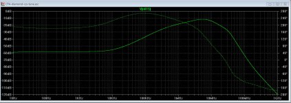
Even this CFA with > 1000V/µs and a 8MHz bandwidth has a 10KHz open loop bandwidth.
http://www.esperado.fr/vssa-diamond/dvssa.php
The image show the response curve at the input of the VAS in closed loop.
(And, yes, it pass the spladski's test in simulation ;-)
It seems strange, at first sight, to say that modern active devices with FT around 10 or 30 MHz are not fast enough for audio, but it is , alas, reality.
Some can try to reduce the global feedback, using local or nested ones. On my point of view, it don't gives so good results in listening. (Damping factor ?)
Alas, despite all my personal attempts, I am not able to achieve this with power amplifiers, keeping feedback high enough to get decent damping factors and low distortion.
Even this CFA with > 1000V/µs and a 8MHz bandwidth has a 10KHz open loop bandwidth.
http://www.esperado.fr/vssa-diamond/dvssa.php
The image show the response curve at the input of the VAS in closed loop.
(And, yes, it pass the spladski's test in simulation ;-)
It seems strange, at first sight, to say that modern active devices with FT around 10 or 30 MHz are not fast enough for audio, but it is , alas, reality.
Some can try to reduce the global feedback, using local or nested ones. On my point of view, it don't gives so good results in listening. (Damping factor ?)
Attachments
Last edited:
So now a proposition - Spladski's test (part A)
1. The nominal gain of the the amp is 26dB for example and it is stable.
2. Now increase the the feedback by 10db or a factor of 3 without altering any component other than gain setting to make the gain 16dB. You can do this via sim or the real thing.
3. Is it still stable?
Spladski's test (part B)
1. Reduce the gain further to a total of 20db more feedback
2. Is it still stable. If so, you now have your 'factor of 10 goodness'
You have to consider the uncompensated gain bandwidth of the voltage stages which is many times greater than the output buffer stage.
The output stage is relatively sluggish because power devices have to turn on and off and turn off and are subject to delay through a need to clear out the base area of the chip of stored charges before the device can be turned on again.
There are limits to what is achievable in this regard and I selected a -3dB frequency of 1 MHz as an example of a power output stage.
As mentioned in my previous post phase shift starts a decade below that -3dB frequency point, at 100 kHz in my example. These parameters cannot be changed by negative feedback.
I also mentioned a general yardstick solution of limiting the upper -3dB frequency of the Vas (voltage amplifier stage) to that 100kHz level - whereby the Vas stage would align with the output stage before the latter is affected by phase shifts. That would involve deploying a lag capacitor of appropriate value around the Vas stage to make the response 3dB down at 100kHz.
A characteristic of gain bandwidth products is that gain and bandwidth are inter-related. Where the closed loop gain is reduced to increase the feedback factor, there is a consequential increase in the closed loop bandwidth in the Vas stages which will now cross beyond the 100kHz previous phase margin threshold.
While possible to alter the compensation to bring things back in line, an increase in feedback factor involves a reduction in attenuation of the feedback signal, increasing the magnitude of the signal reaching the inverting input terminal.
If the common mode signal level reaches 1-2 volts R.M.S. this can be the dominant distortion mechanism due to modulation of the inverting transistor base width varying according to the base emitter voltage. This is another case of something that cannot be mended with negative feedback.
If the values of lag capacitors have to be increased then the loading on the current draw of the input and Vas stages has to be investigated.
I don't like.
?The output stage is relatively sluggish because power devices have to turn on and off and turn off and are subject to delay
Thanks,
Amended version
The output stage is relatively sluggish because power devices have to turn on and off. These are subject to delay through a need to clear out the base area of stored charges to turn off the device before it can be turned on again.
Last edited:
What surprised-me was the word "delay". The charge of a condenser by a voltage don't delay a signal, it starts at the exact moment the voltage is applied.The output stage is relatively sluggish because power devices have to turn on and off and are subject to delay through a need to clear out the base area of the chip of stored charges before a device can be turned on again.
Spladski, what do you think, do I get it right straight off the bat? Never, not once in my life did I construct anything that worked perfecty as is, and that is the part of the whole I enjoy the most, bringing it back home by adjusting and readjusting until it does what it's supposed to do, the way it's supposed to be done. The really fun part is the developement of the initial model.
It hasn't been just once that a problem here was solved by changing something there, sometimes to my suprprise. That's the fun of it.
It hasn't been just once that a problem here was solved by changing something there, sometimes to my suprprise. That's the fun of it.
What surprised-me was the word "delay". The charge of a condenser by a voltage don't delay a signal, it starts at the exact moment the voltage is applied.
There is a delay , not of electrons .... they move an inch a minute.
In a vacuum the EM wave is the speed of light , copper is half of this.
Various semiconductors even less.
So . "exact moment" would be the speed of light. Semi's and most passives
fall far short of this ... there has to be some true delay.
OS
Thanks,
Amended version
The output stage is relatively sluggish because power devices have to turn on and off. These are subject to delay through a need to clear out the base area of stored charges to turn off the device before it can be turned on again.
True. However, there are well known techniques to deal with this, a speedup capacitor is just one of them.
This was and is much more of a problem with low and medium Ft devices, such as MJ15xxx and MJ211xx series, but the current crop of output devices, such as NJW and so forth are inherently much faster, approximately 5 times as fast as the MJL devices. Therefore, the problem while not eliminated has been much reduced.
Lastly, a good way to mitigate the problem is to run the output devices at higher bias currents, not the Japanese typical 20-30 mA per device, but at 120-140 mA per device. Effectively, they never turn off completely, but this method does its work by shortening the on/off window and typically eliminates crossover distortion by a wide margin. The downside is having to use bigger and better heat sinks to be able to sustain the qiuescent bias current and keep it from overheating the heat sink.
This method also works very well with older, slower power devices of the whole MJ and MJL series.
What surprised-me was the word "delay". The charge of a condenser by a voltage don't delay a signal, it starts at the exact moment the voltage is applied.
Increasing currents exacerbate stored charge effects - another term is Carrier storage - described in Dictionary of Electronics by S.W. Amos and R.S. Amos - as: "An effect in PN junctions which have been driven hard into conduction whereby the current continues to flow for a brief period after the applied voltage has been removed. More majority carriers move towards the junction than are needed to supply the external current: these are stored and are able to continue the current briefly when the applied voltage is reduced to zero."
In output stages where the driver transistors are cross coupled by a resistor connection between their emitters, the output devices are reverse biased on opposite cycle swings to drain out stored charges. This is a good thing since it helps the switching process. Nonetheless phase shifts will arise from this and capacitive and inductive effects associated with the transistor devices and wiring.
Any concern with analog audio signals at <10MHz and the lengths we use ?There is a delay , not of electrons .... they move an inch a minute.
In a vacuum the EM wave is the speed of light , copper is half of this.
Various semiconductors even less.
Last edited:
I showed a Rotel amplifer this week . Looking at the VAS or TIS it doesn't have the standard capacitor from collector to base ( Cdom CB ). Instead as not well liked in Self it is a cap and resistor collector to ground. Stan Curtis and Mike Balance ( yep, how suitable and a real gentleman ) were not idiots. I have experimented with a split CB cap and injected crossover distortion into the split node. MOS FET's have a little at 50 kHz and it will remove it. A feedback pair showed no advantage. I like MOS FET's. It is an easy way to get the best of both worlds. Stability is seemingly unchanged. The often critised Cdom is rather wonderful. BTW. Single input stages are not remarkably better as some will have it. Some old amps had transistors with very high capacitance. They don't need Cdom. It is not a great idea to do that. A NPO ceramic is a better capacitor.
I have seen Cdom extended over more sections. I doubt it helps.
I have read that marginally unstable amps sound better. This seems very possible. The question is could the music make it happen ? Possibly not.
One thing I have struggled with is should the VAS be a VAS or TIS ? I think I have an answer. Dejan ( DVV ) uses a VAS. That is he has an impedance lifting emitter resistor in the VAS. Lets say 47R and 8 mA. Just like Cdom this is Rdom. If the transistor has gain of 100 and re is 25/8 or abour 4R Zin in is 400R ( 8 mA ). With Rdom more like 5 K. If using a standard simple LTP input stage and say a generous 2 mA tail current we are looking at 620R or 1K into VAS version. One has a transfer ratio of 0.8 and the other 5. I have a hunch this matters. At the risk of some 2nd harmonic the resistor can be set low. I would say 2nd in correct propotion is good. This argues against a current mirror. In my opinion slew rates are mistaken. All they are is this problem VAS/TIS solved. That is use a VAS. Twin VAS is better as it simplifies the problems if a network is placed in VAS 1 to mimic the output stage.
If lests say a BC 550C is used with perhaps a MPSA 42 in cascode we might get this, re = 4 x u=500 = 2K . Now if that is fed from 620R or a current mirror we are onto a winner. My tests with cascode say it is just one transistor in terms of stability. If seeking linearity bias your cascode generously ( Early effect ? ). You can still split Cdom if you choose. With this in place I doubt I would fit Rdom. Amplifiers with Rdom = 0R seem to sound tighter which isn't a mystery I guess ? BTW have your driver stage clip first. It sounds nicer. No one needs that extra 25 watts when already 200 watt 4 R. You can have a switch if it bothers you. If so have + 10 V power rails and pure DC.
My prefered output stage is MOS FET. 2 sets of FET is no bad idea as then Ron is like generously degenerated biopolar stages. 8 mA will drive two sets to Bat frequency levels of output. As we said about diodes yesterday I just love that MOS FET's need a resistor and nothing else to bias them. No curve distortion there.
Talking of Bats. The tweeter in my girlfriends speakers goes to > 45 kHz ( - 3 db ). I roll it off at 24 Hz, it retains it's speed. It is easy to hear it is rolled. I can not hear above 16 kHz which is OK for 60, still can hear what the tweeter has ( wave shape, not spot frequency ). The dog can hear it. When playing 1960's 45's the dog had it's paws over it's ears! Joe Meeks Telstar was excellent. BYTW. The more open the sound and more gentle the easier it is to ignore record damage.
Just off to Loricraft now . Using my Magneplars as the OB being stripped for a coat of paint and Danish oil to the ply ( Loricarft workshops ). Am being filmed by a private TV company who is ex marketing man from JVC and my mate Paul Stewart. We have Brian Mortimer who was head of Quality control at Garrard being filmed. His dad invented autochagers and the 301 . Paul, JVC TT71 is the only turntable after my own 401 I lust after. 501 is silly money, even though I designed it I can't have one. A JVC L3-E eat my stand in LP12 Ekos for breakfastk. L3-E is a TT 71 more or less. The crap arm is not crap sounding nor AT clone pick up. L3-E is the girl in the film who half way through turns out to be beautiful. No cogging or kidding.
Nige, I told you many times - Douglas Self should not be your reference because he's simply too biased. I mean, we all prefer this to that, but not many of us are as exclusive as he is.
On that VAS - do take a look at Samuel Grobner's site for what I feel is the best solution overall. Not perfect, but the best compromise all around.
On output MOSFETs - I stand by my original view, using say IRF 240/9240 devices, they do the job, but to me, they still don't sound quite right. Personal taste - quite probable. I find their bass lines to be lacking in substance.
Last edited:
- Status
- Not open for further replies.
- Home
- Member Areas
- The Lounge
- Sound Quality Vs. Measurements