Hello,
The standard light bulb can not be used for the exposure.
But, if you can't find the UV lamp, it is possible to use the 500 - 1000 W halogen lamp (reflector).
Try at distance of 30 cm, 45 sec. (500 W)
Note that you must use the glass over the film, and that some heat will be dissipated from the halogen lamp.
Regards,
Kristijan Kljucaric
chorei said:what is the difference between UV and IR lamp when doing PCB exposure ?
The photo lack is sensitive for UV light, usually (I mean the Positiv 20 spray).
The high power halogen lamp can be ok also, I agree with Kristjan.
BR,
Milan
Hello,
Yes, the precise amount of NaOH in the water depends on photoresist manufacturer and of photoresist age.
The period of developing is also depends on precise amount of NaOH in the water, photoresist manufacturer, photoresist age and how well is done the exposure of photoresist.
So, you must done some visual checking when developing your artwork.
Use room temperature solution of NaOH and water.
Kristijan Kljucaric
http://web.vip.hr/pcb-design.vip
Hello trigon,
The gold plating of the PCBs is possible, but it is just unneccesary to make them that way, and the cost is not justified.
There is no way to get any better sound results with the gold.
The main purpose of plating the PCBs is to protect the Cu tracks and pasds against corosion - oxidation, for improved solder joints when soldering thus lowering joint resistance.
Also, there is much less risk for cold joints.
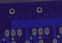
On my PCBs I use Pb-Zn track overlay.
I enclosed the picture, and like you can see, the silver look of the pads are achived by tinplating.
The all tracks are tinplated, even under blue soldermask.
Best regards,
Kristijan Kljucaric
http://web.vip.hr/pcb-design.vip
The gold plating of the PCBs is possible, but it is just unneccesary to make them that way, and the cost is not justified.
There is no way to get any better sound results with the gold.
The main purpose of plating the PCBs is to protect the Cu tracks and pasds against corosion - oxidation, for improved solder joints when soldering thus lowering joint resistance.
Also, there is much less risk for cold joints.
On my PCBs I use Pb-Zn track overlay.
I enclosed the picture, and like you can see, the silver look of the pads are achived by tinplating.
The all tracks are tinplated, even under blue soldermask.
Best regards,
Kristijan Kljucaric
http://web.vip.hr/pcb-design.vip
Attachments
Hello,
It is a not good idea to leave photoresist on board after etching.
It will be hard to solder components, and there is much more risk for bad or cold joints.
Remove the all photoresist with the some solvent and try to put tin layer of solder over the all tracks.
That way it will be very easy to solder the components, and the tracks will have the protection against corosion-oxidation.
Best regards,
Kristijan Kljucaric
http://web.vip.hr/pcb-design.vip
Hi all,
I am currently thinking of making my own PCB using Photoresist method and negative sentised boards from Kepro and run into a few questions:
1. Does anyone know how to turn the PCB artwork in Protel into negative PCB artwork directly in computer before print out on the laser/injet printers (setting? configurations?) ? I know I can use Kepro's Photo Reversing Kit but it's just too expensive as I only have 2 6x4 boards to make.
2. If I can't turn the PCB artwork into negative easily, any other Copper Clad manufacturers or methods you can recommend?
Thank you in advance for all of your help,
Andy
Its depends on which version of protel you are talking about.
But in the case of protel 98, in the printer properties you have an option to print out either the pcb layers or as composite of the pcb.
Choose composite and go into options and turn off the layers you don't want.
In there ,there is an option to mirror to artwork.
Its been a while since I have used protel 98. I am planning on developing a pcb for the X-SE Amp so I will be loading Protel 98 again soon. If you need any more help let me know I've been using Protel for years...
Regards
Anthony Holton
Banned
Joined 2002
Hi Anthony,
Thank you for the fast reply. What I wanted to do is to "invert" the PCB artwork, specifically, turn all the black traces into white and all the white space in the board into black to generate negative so I can expose the negative sensitised boards. Please help if you know how to. Thank you.
Thank you for the fast reply. What I wanted to do is to "invert" the PCB artwork, specifically, turn all the black traces into white and all the white space in the board into black to generate negative so I can expose the negative sensitised boards. Please help if you know how to. Thank you.
Hello acliao,
Why not use just the the PCBs with the ordinary - positive sentised photoresist ?
Much less trouble and same results.
Best regards,
Kristijan Kljucaric
http://web.vip.hr/pcb-design.vip
Why not use just the the PCBs with the ordinary - positive sentised photoresist ?
Much less trouble and same results.
Best regards,
Kristijan Kljucaric
http://web.vip.hr/pcb-design.vip
- Status
- Not open for further replies.