Professional made PCBs for Aleph series amplifiers and for some other DIY audio projects.
http://web.vip.hr/pcb-design.vip
Also, custom made PCBs are possible for 5 PCBs and up.
http://web.vip.hr/pcb-design.vip
Also, custom made PCBs are possible for 5 PCBs and up.
Here's another source for some Pass designs.
http://www.audioxpress.com/bksprods/pcbs/zen.htm
BUT I have to say that the layout on the
Kristijan boards is mighty pretty
http://www.audioxpress.com/bksprods/pcbs/zen.htm
BUT I have to say that the layout on the
Kristijan boards is mighty pretty
For your information ....
www.audioXpress.com do NOT sell Pass Labs Aleph series boards ........ if they do, we won't have to go through this exercise of creating boards from scratch or search all over the world for it!
www.audioXpress.com do NOT sell Pass Labs Aleph series boards ........ if they do, we won't have to go through this exercise of creating boards from scratch or search all over the world for it!
I bought the Balenced Zen Line Stage boards from AudioXpress, and they are nicely done. Very clean boards.
--
Brian
gte619j@prism.gatech.edu
--
Brian
gte619j@prism.gatech.edu

Hello Strobo,
The Aleph 5 and the rest PCBs are made of 1,6 mm fiberglass base with Cu-50 mikron + Pb track overlay, two sided dark-blue soldermask, drilled, and with white component overlay.
The all PCBs are single sided.
-------
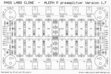
Actually, I finished PCB for Aleph P Version 1.7 and the size is :
215 mm x 125 mm (8,5 in x 5 in).
The PCB layout is similar to other PCBs that I designed on my homepage, and it is very simetrical.
There is one PCB for two channels, like for Balance Line Stage.
Regards,
Kristijan Kljucaric
The Aleph 5 and the rest PCBs are made of 1,6 mm fiberglass base with Cu-50 mikron + Pb track overlay, two sided dark-blue soldermask, drilled, and with white component overlay.
The all PCBs are single sided.
-------
Actually, I finished PCB for Aleph P Version 1.7 and the size is :
215 mm x 125 mm (8,5 in x 5 in).
The PCB layout is similar to other PCBs that I designed on my homepage, and it is very simetrical.
There is one PCB for two channels, like for Balance Line Stage.
Regards,
Kristijan Kljucaric
Hello Strobo,
If you look at the bottom of the PCB (track side) you will see that some PCBs have green color over the tracks.
This is soldermask.
Instead of green, I use blue soldermask.
At my PCBs, the soldermask is double sided, one layer is on the track side of the PCB, and other layer is on component side - before white component overlay.
I use it on the component side just to get better contrast of white silkscreen (component) overlay.
----------
The Aleph P 1.7 preamplifier will be posted at: http://web.vip.hr/pcb-design.vip in a couple of hours.
Regards,
Kristijan Kljucaric
Attachments
Hello,
You asked me a question that I don't know to answer very well on english.
But, I think you will understand.
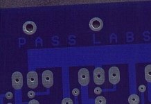
The Pb track overlay on the mine PCBs is a tin layer of Pb/Zn over the Cu tracks.
I think that the right word on english would be - Tinplated.
I enclosed the picture, and like you can see, the silver look of the pads are achived by tinplating.
The all tracks are tinplated, even under blue soldermask.
Tinplating serve for protection from the oxidation of the Cu tracks/pads, thus for improved joints when soldering and lovering the joint resistance.
Also, there is much less risk for cold joints.
Hoped I answered your questions.
Regards,
Kristijan Kljucaric
You asked me a question that I don't know to answer very well on english.
But, I think you will understand.
The Pb track overlay on the mine PCBs is a tin layer of Pb/Zn over the Cu tracks.
I think that the right word on english would be - Tinplated.
I enclosed the picture, and like you can see, the silver look of the pads are achived by tinplating.
The all tracks are tinplated, even under blue soldermask.
Tinplating serve for protection from the oxidation of the Cu tracks/pads, thus for improved joints when soldering and lovering the joint resistance.
Also, there is much less risk for cold joints.
Hoped I answered your questions.
Regards,
Kristijan Kljucaric
Thank you Kristijan,
You explained that to me very well.
Now I understand everything about your PCBs.
Well, almost all.
At Passdiy gallery I founded your SIGMA 6 preamplifier.
Why you used the separate PCBs for the left and right channels ?
Why the PCBs in your SIGMA 6 preamplifier are not silkscreened ?
You explained that to me very well.
Now I understand everything about your PCBs.
Well, almost all.
At Passdiy gallery I founded your SIGMA 6 preamplifier.
Why you used the separate PCBs for the left and right channels ?
Why the PCBs in your SIGMA 6 preamplifier are not silkscreened ?
- Status
- Not open for further replies.