Hi Mike, Andrew,
Thank you for your care.
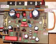
I made a small experiment with a help of a small piece of ice cube covered in a plastic bag and placed over all bjt peers. Definitely second LTP is the culprit for thermal runaway ... actually is not a true runaway, is only a very slowly bias stabilization (30-40min). What is worse is bias sensitivity at cold air, it decrease very sharply at a small airflow like an open window or a person running in my lab room - Andrei, my 3 years old child

The VAS LTP Vce at cold is 710mV and after warming up 690mV.
Thank you for your care.
I made a small experiment with a help of a small piece of ice cube covered in a plastic bag and placed over all bjt peers. Definitely second LTP is the culprit for thermal runaway ... actually is not a true runaway, is only a very slowly bias stabilization (30-40min). What is worse is bias sensitivity at cold air, it decrease very sharply at a small airflow like an open window or a person running in my lab room - Andrei, my 3 years old child
The VAS LTP Vce at cold is 710mV and after warming up 690mV.
Attachments
jacco vermeulen said:Mihai,
don't you agree that you end up in Tokyo if you need something with better than 300MHz, 2.5pF, 500 hFe and low noise ?
Yes Mr. Vermeulen,
Here in Romania is very hard to get most of the Japanese BJTs, same like the silver mica caps
Where is located your source of such yummies?
roender said:The VAS LTP Vce at cold is 710mV and after warming up 690mV.
I guess you meant Vbe? This is a 3% variance... The Vbe values set the bias in 2nd stage.
What are your differences in outputstage bias?
Mike
Hi,
Vbe~=650mV and Vce=690 to 710mV.
Does that mean the VAS are saturated?
If so then you will be getting wierd characteristics.
I would reset the cascode reference to give at least 2Vce or maybe as high as 5Vce.
BTW,
what you are describing does not sound like hFE variation, more like Vbe variation with temp. Again abolutely normal for all transistors.
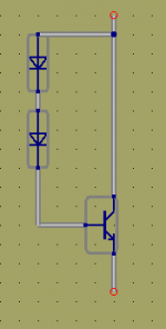
Maybe just try connect anode of D8 to LTP emiters instead VCC.
By the way.. this configuration always look very risky for me. If voltage
on R18 is so low, then small change VBE (due to temperature drift for
example) can largely change VAS bias. Mayby do as MikeB suggested: replace R18 with ccs?
By the way.. this configuration always look very risky for me. If voltage
on R18 is so low, then small change VBE (due to temperature drift for
example) can largely change VAS bias. Mayby do as MikeB suggested: replace R18 with ccs?
 CCS for R18. R21 & R22 are the reference for the second diff emitter voltage. Loose D6 & D7.
 If you tied R21 & R22 to the emitters of the second diff instead of the positive rail, with a CCS for R18, there would be no voltage reference for the emitters and it will fall out of bias. Now if you then use a P-channel J-fet, with a source resistor to the positive rail, gate to the emitters of the second diff, and the drain to the source resistor on J3 to control the bias current of the first diff to bias correctly the second diff in sort of a common mode bias feedback loop. Both differentials' bias currents would then be referenced to the source current of the CCS in place of R18. Do you guys think this approach could achieve better CM operation and bias stability? Opinions?
CBS240 said:
D6/7 can't be skipped, without them the 2nd diffamp would enter badly reversebias when amp clips.
A high CMRR is not needed for 2nd diffamp as it is fed balanced by first diffamp, creating minimal voltage changes to r18 during normal operation.
Roender, have you already measured vbe variance in 2nd diffamp?
How big is the bias change in vas? (simply measure V across r18)
"bias variance in outputstage is 40-45mA", does that mean bias in outputstage varies by 40ma, or between 40-45ma?
Most of the amplifiers have a vas bias dependent on the Vbe of the vas devices, typically even much stronger than here, using emitter resistors to vas devices much smaller than 68ohm.
A ccs shouldn't be necessary here.
Maybe the outputstage is too sensitive to vas bias variation?
My suggestions:
- try a diode in series to the LED, this will increase Vce to the diffamp devices by 0.6v, maybe they are too close to Vce-sat
- try 2n5401 instead of bc560c, you don't need very high hfe here.
Mike
MikeB said:
My suggestions:
- try a diode in series to the LED, this will increase Vce to the diffamp devices by 0.6v, maybe they are too close to Vce-sat
Mike
But we will loose some output swing voltage ...

roender said:Variation over VAS 68ohm tail resistor:
275mV ~ 4.04mA at room temperature
343mV ~ 5.04mA hot
LTP current variation (on negative rail CCS)
4.77mA at room temperature
5.03mA hot
I_final stage variation (on a single pair of final devices)
75mA cold
119mA hot
The variation in 1st stage is bad... That changes the output from 1st stage, changing bias. ~0.15ma over 470ohm gives a change of ~70mv, quite exactly the bias drift you measured at r18...
Looks like the 2bjt-ccs was a better choice here. (the sensing bjt keeps cold having vce of ~1.2v, heating it up even lowers the current supplied)
The variation at output from 1st stage in my symasym was ~1-2mv... thats ~30 times less.
Can you confirm that by measuring r21/22?
Mike
MikeB said:
Can you confirm that by measuring r21/22?
Mike
The voltage over r21/22 is 925mV at room temperature (1.968mA) and 960mV after the amp became warm (2.043mA) => deltaV=35mV
This is only one part of the problem because the LTP CCS has a short settle time, 1-2min.
The other part of our problem is in VAS LTP. BC560c has a very sensitive hfe/Vbe with temperature
Hi Mike,
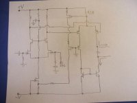
Sorry for trying to change your circuit around, that was bad form. You are correct that a CCS is not really needed. However, I wonder if using an active bias would correct for the changes in temperature. In this simplified sketch, the idea is to balance the bias currents of both LTP's on Vgs of the p-channel j-fet (I X R18) with a control loop so that if Hfe and Vbe change with temperature, the p-channel j-fet adjusts the bias source of the first LTP to correct the voltage across R21 & R22 to maintain a constant current in the second LTP regardless of Vbe. Choose a source resistor so the j-fet will self bias across R18, at the point where the transfer characteristics have no change in Vgs vs Id with regard to temperature. The j-fet's temperature would not change as much anyway and thus both circuits' bias would not be as temperature dependent. All this may be valid...
Of course then agian, I might just have had too many beers, eh?
Attachments
Did You sad :"The VAS LTP Vce"? if that means Q8 and Q9 Vce, then their Vbe or beta variations has not much to do with their Vce, which is determined by Q14, Q16 and D8.
A second thing: D4 and D5 has large dynamic resistance. If you use some kind Vbe-multiplier (Vd4 and Vd5 dependent), then output stage bias will be much less depend on VAS bias.
A second thing: D4 and D5 has large dynamic resistance. If you use some kind Vbe-multiplier (Vd4 and Vd5 dependent), then output stage bias will be much less depend on VAS bias.
Attachments
- Status
- This old topic is closed. If you want to reopen this topic, contact a moderator using the "Report Post" button.
- Home
- Amplifiers
- Solid State
- Searching for high hfe, low noise and cob PNP BJT