Hi
You have probably already thought of this but here goes. All I do with the BC 550 and BC 560 is to press them against a common heat sink to keep the temperature low and constant.
My "special " transistor for preamps and low noise is the lm394 ( in a can ) which does may meet all your needs but it is excellant.
Don
Hi,
all silicon transistors have a similar Ic vs Vbe characteristic that varies markedly with junction temperature.
I think hFE has the same variation with temp.
These variations are normally reduced by using an LTP to balance out changes.
Even better balance is achieved by thermally coupling the devices and better still with a dual device.
Hi Roender,
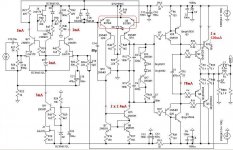
what is D1? a Zener or a 1mA CCS?
your output stage currents seem astray.
70mA through R5 generates 1.54V.
The bias across the emitter resistors will be about (1.54-1.3)=0.24V this generates Iq=2.4A.
Reduce Ir5 to about 61mA and the bias reduces to about 420mA , Vre~=21mV. Iq=2*[(22r*0.07A)-1.3V]/(0r1*2)
Note how sensitive Iq is to small changes in Ir5.
How will you adjust Vbias? 4diodes will not achieve accuracy. Are any on the output heatsink for temperature compensation?
You have cascoded the second LTP and achieved good HF response then killed that response by fiiting a Miller comp cap. Why have you fitted C14 to the collector of q10 rather than the collector of Q16?
Why have you fitted R12 & R13?
Tomahauk,
connect those transistors?
Do you mean match their parameters?
Hi,
your choice of values for C19 & C21 produce RC time constants near 220mS.
If you adopt the philosophy of setting the PSU RC to half an octave above this (330mS) then you are forced to adopt +-40mF/channel for 8ohm speakers and +-80mF/ch for 4ohm speakers.
Is C19 in series with a DC blocking cap in your source?
The combined RC of the input could usefully be reduced to 80mS and still retain good bass response. Then C21 can be reduced to 220uF and that allows smoothing to be reduced by half.
The input filters should set the frequency response of you amp. All the internal circuitry should exceed the bandwidth of the filters by a margin, that you select.
AndrewT said:4diodes will not achieve accuracy. Are any on the output heatsink for temperature compensation?
Hi Andrew, Roender uses NJL-output devices, they have built in diodes.
Mike
AndrewT said:Hi Roender,
what is D1? a Zener or a 1mA CCS?
your output stage currents seem astray.
70mA through R5 generates 1.54V.
The bias across the emitter resistors will be about (1.54-1.3)=0.24V this generates Iq=2.4A.
Reduce Ir5 to about 61mA and the bias reduces to about 420mA , Vre~=21mV. Iq=2*[(22r*0.07A)-1.3V]/(0r1*2)
Note how sensitive Iq is to small changes in Ir5.
How will you adjust Vbias? 4diodes will not achieve accuracy. Are any on the output heatsink for temperature compensation?
You have cascoded the second LTP and achieved good HF response then killed that response by fiiting a Miller comp cap. Why have you fitted C14 to the collector of q10 rather than the collector of Q16?
Why have you fitted R12 & R13?
Hi Andrew
First thing first, the schematic is derived from MikeB symasym, thank you Mike.
D1 is a 12V zener connected as a cascode reference voltage and as a load for 1mA CCS (upper one)
R5 is 15ohm in reality, 20ohm in LTspice to achieve the same driver current as in reality.
R35 is a 500ohm trimpot connected in parallel with 220ohm metal film resistor.
Two NJL (ThermalTrack) diodes are connected in series with two BE junction (5551/5401) for properly bias tracking.
C14 is not a miller cap, is more like phase lead compensator and it helps to stop HF ringing. The voltage developed across this capacitor has very little variation, in range of 1-2V
R12 and R13 are no longer in use, was a wrong way to liniarize the VAS stage
AndrewT said:...
Tomahauk,
connect those transistors?
Do you mean match their parameters?
i mean thermal connection, for example glue them (the easiest) or gird them with metal clamp, then parameters will change the same in both of transistors (junctions will have almos the same temp in both transistors)
Attachments
AndrewT said:Hi,
your choice of values for C19 & C21 produce RC time constants near 220mS.
If you adopt the philosophy of setting the PSU RC to half an octave above this (330mS) then you are forced to adopt +-40mF/channel for 8ohm speakers and +-80mF/ch for 4ohm speakers.
Is C19 in series with a DC blocking cap in your source?
The combined RC of the input could usefully be reduced to 80mS and still retain good bass response. Then C21 can be reduced to 220uF and that allows smoothing to be reduced by half.
The input filters should set the frequency response of you amp. All the internal circuitry should exceed the bandwidth of the filters by a margin, that you select.
Andrew,
Now you lost me ... I have no DC blocking cap in DAC output.
How this will solve my problem?
Tomahauk
All BJT peers are thermaly bounded
Best regards,
Mihai
Hi Roe,
no need to feel lost in this community.
The NFB is set too high for this and I suspect the PSU will be at least an octave too high and maybe 2 or 3 octaves too high.
The rule seems to be that:-
bandwidth is set by input filter.
The NFB turn over frequency should be at least half an octave below the input filter.
The PSU effective turn over frequency should be at least half an octave below the NFB F-3db.
If you want extended low low bass I recommend that F-3db should be a full decade below 20Hz i.e. below 2Hz.
To match this NFB should be below input F-3db/1.4
and PSU should be below NFB F-3db/1.4
take an example
set input HP filter to 90mS (1.7Hz)
NFB=140mS
PSU=200mS This requires +-25mF/ch for 8ohm speakers.
no need to feel lost in this community.
If the 10uF is the sole DC blocking cap then it sets the high pass filter. That 10uF value and 22k input impedance set the -3db of the high pass to 0.7Hz.The input filters should set the frequency response of you amp. All the internal circuitry should exceed the bandwidth of the filters by a margin, that you select
The NFB is set too high for this and I suspect the PSU will be at least an octave too high and maybe 2 or 3 octaves too high.
The rule seems to be that:-
bandwidth is set by input filter.
The NFB turn over frequency should be at least half an octave below the input filter.
The PSU effective turn over frequency should be at least half an octave below the NFB F-3db.
If you want extended low low bass I recommend that F-3db should be a full decade below 20Hz i.e. below 2Hz.
To match this NFB should be below input F-3db/1.4
and PSU should be below NFB F-3db/1.4
take an example
set input HP filter to 90mS (1.7Hz)
NFB=140mS
PSU=200mS This requires +-25mF/ch for 8ohm speakers.
Hi Roe,
I see now you were referring back to the initial question.
Solve what is wrong with the amp before blaming the variable hFE. As said before ALL transistors suffer from variable hFE and all amplifiers should be designed to be substantially impervious to variations in this parameter.
Sort the amp, instead of looking for perfect transistors that don't exist.
Would you care to comment on the philosophy of matching the RC time constants as described? I am always open to modifying my beliefs/recommendations particularly if backed up by contrary, but well argued, evidence.
you asked a question, I answered it.Now you lost me ... I have no DC blocking cap in DAC output.
How this will solve my problem?
I see now you were referring back to the initial question.
Solve what is wrong with the amp before blaming the variable hFE. As said before ALL transistors suffer from variable hFE and all amplifiers should be designed to be substantially impervious to variations in this parameter.
Sort the amp, instead of looking for perfect transistors that don't exist.
Would you care to comment on the philosophy of matching the RC time constants as described? I am always open to modifying my beliefs/recommendations particularly if backed up by contrary, but well argued, evidence.
AndrewT said:Sort the amp, instead of looking for perfect transistors that don't exist.
Would you care to comment on the philosophy of matching the RC time constants as described? I am always open to modifying my beliefs/recommendations particularly if backed up by contrary, but well argued, evidence.
Andrew, about the RC times, i choosed that input filter in the original symasym because it seemed the best compromise between bandwidth and linear inputimpedance up to ~20khz. Symasym can be forced to slewrate limits with inputsignal, but seemed to be no problem.
About the highpass, that's my fault, i always forgot to adjust it.
About the cause of the unstable biasing, i don't know what causes it here, the original symasym has very stable biasing. I suspect that the very low Vce (caused by the cascodes) to the devices in 2nd diffamp causes large variations in vbe from thermal changes. In the worst case you have to replace the 68ohm by a ccs.
On the other hand, with that low Vce, how can these devices heat up?
Roender, are you sure that these 2 transistors are the problem, and not surrounding parts like cascode/LED ? Have you measured VCE to the LTP devices?
Mike
- Status
- This old topic is closed. If you want to reopen this topic, contact a moderator using the "Report Post" button.
- Home
- Amplifiers
- Solid State
- Searching for high hfe, low noise and cob PNP BJT