Hello,
I am currently trying to modify a JLH mosfet amplfier. This was designed back in '82.
What I am trying to do is replace Q10 which is a VN1210M (1w) vas fet with a higher power VN1210D device. (45w). Obviously the VAS CCS and vbe transistors will have to be upgraded and probably heatsinked. Enno Borberly in his earlier designs such as the DC100, Servo 100 etc recommend driving lateral Mosfets with about 30-40mA per pair. This was because of the capacitance, apparently this improves HF THD and also the slew rate. Another thing that JLH does in his design is uses different gate resistors (presumably to match the bandwidths closer). But I would prefer to use equilisation capacitors over the N Chl mosfets as I do not think the slew rates could be symmetrical ?? (not sure on that one)
My questions is, can I replace the VN1210M with a higher power VN1210D and will this affect the compensation of the amp ie. need different compensation capacitors etc. I am not good enough to adjust this to be honest.
I have included a link to a datasheet which shows the devices in question. One minor problem is that it does not show the VN1210M by name.
Just wondered if anyone had any old supertex databooks with these devices in particular. Think I am alright though.
http://pdf.alldatasheet.com/datasheet-pdf/view/25955/SUTEX/VN1210D.html
Any help appreciatted
Kevin
Attachments
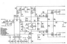
Thanks for schematic Kevin 
We are discussing JLH 80 Watt MOSFET in another topic
and did not know where to find a schematic for this amp.
Suddenly you posted this thread!
Your schematic was really 'heaven sent'.
see this topic:
Effect of Power Supply on Soundstage Width
Another guy, foxyb, is modifying his JLH 80.
We are discussing JLH 80 Watt MOSFET in another topic
and did not know where to find a schematic for this amp.
Suddenly you posted this thread!
Your schematic was really 'heaven sent'.
see this topic:
Effect of Power Supply on Soundstage Width
Another guy, foxyb, is modifying his JLH 80.
Kevinbd said:I am currently trying to modify a JLH mosfet amplfier. This was designed back in '82.
Just to avoid any possible confusion for people reading this thread, the schematic you have posted is not the circuit that was published in Wireless World in August 1982 (80-100W MOSFET Audio Amplifier). It is the schematic for the later 'Audio Design Amplifier' which appeared in the July 1984 edition of ETI.
JLH 80W amp
Hi Kevin,
I have the Supertex Databook dated 1991, but the 'M' suffix VN1210 device is not shown in this either!
However, from the book it is clear that with these various VN1210 Supertex family devices, provided there is merely one letter in the suffix (i.e. 'M', or 'L', or 'D') there are no differences as far as their electrical parameters go. The differences here are merely their packages and therefore their power ratings/heat dissipations etc.
Where there is a number added to the suffix as well as the following letter (i.e. VN1210N2, VN1210N5 etc.) this no longer holds true, and their electrical parameters are different.
As the 'D' suffix devices you mention are T0-220 packages, it would seem that they will be fine in the intended application.
The original 'M' suffix Mosfets (I have some to hand) are merely the size of a TO-92 with a small metal tab on top (I have not come across these devices before, nor since, so I don't know what the packages are called!) but their dissipation will be much less than a T0-220.
You mention the gate-stopper resistors, R18/19 & R21/22, and you are correct in your assumption that R18/19 are higher values than R21/22 to 'balance' the different capacitances of the output devices, to bring the HF roll-off points nearer to each other.
You may also be interested to know that the designer later recommended that these be increased to 330R for R18/19, and 270R for R21/22.
I hope this helps.
Changing the negative feedback resistors
Hello,
Lineup quoted the following on another post about soundstage width.
"The gain is slightly less than (150k / ( 0.82k + 2.2k // 0.5k ))+1
Would make <123.2 or <41.8 dB, because impedance of C7, 9uF4 is not zero."
My question is can the NFB impedance resistors be scaled down. The reason for this is to reduce the noise and DC offset. I personally do not like the cap & trimmer (RV2 & C8) over the LTP emitters. Plus there is degeneration resistors to consider as an improvement.
Could I change R1, R14 to 75K (to start off with) and change R8 to 410R ?
Would polyprop cap C7 have to be scaled up to 20uF also ? Would like to keep the polyprop cap if possible.
I figured after reading Doug Self's book regarding degeneration that re = 25/0.25 = 100. So if the current is doubled in the tail source I could add 50R or 47R resistors. (I think the pot has to go with degen resistors ? not sure
The only hole in the head to all this is whether stability is radically altered!. Here is a link that discusses the gain being to high for modern sources.
http://www.diyaudio.com/forums/showthread.php?postid=788014#post788014
Best Regards
Hi Fanuc,
The answer to your first question is certainly 'Yes', you can scale the resistors and caps within reason.
In fact the only reason the designer (JLH) used much higher resistors here than previously, was that when he visited me I had demonstrated the sonic improvements to be had when using film caps for DC feedback blocking, in place of original electrolytics.
I had previously tried the much higher than usual 150k for the feedback R14 (which then needed R1 to be increased accordingly to avoid any offset) together with a single 4k5 (in place of the entire 'balance' arrangement) to ground, to enable a 10uF film cap to be used in series here.
I didn't care for this 'balance' arrangement, at least not what it did to the sound, mainly because of the variable pot used here in a very critical part of the circuit as far as 'sonics' are concerned.
The same goes for any electrolytic cap (which I was then aware of) because all of those which I had tried sounded awfull compared with a wire bypass I had also previously tried.
You are also correct in your assumption that if the feedback resistors are decreased in value, to preserve the intended lower cut-off here, you will need to increase the cap's value proportionately to achieve a similar time constant.
This calculation is made using the value of the smaller resistor alone (in my case the 4k5 to ground) and the chosen cap, and not, of course, the higher value feedback R14 which does not affect this issue.
Wishing to achieve a -3dB (lower) cut-off which I thought was suitable here, using a 4k5 resistor which I had to hand, gave me a calculated result in the region of 3 to 4 Hertz (IIRC) when used in series with a 10 uF film cap which I had obtained for this purpose.
I also wished to achieve an overall gain of approx. 35x, so with using 4k5 for the smaller resistor, this required approx 150k for the feedback R14. (150 + 4.5/ 4.5 = 34.33x) None of these choices is really very critical in practice.
There was a potential for slightly more noise as a result of the increase in resistances, but I chose some better quality components here to help offset this, and the overall sonic improvement was sufficiently impressive to JLH for him to adopt this arrangement in future designs.
Incidentally, the output DC offset is mainly governed by the matching of gains of the input LTP, and the closeness in matching of the total resistances from Q1's base to ground (i.e. R1 + R2) and the value of the larger feedback resistor, R14. If these gains and total resistances are exactly equal, theoretically the offset should be approx. zero, and in my case, I ended up with far less than 10mV in both channels.
I also got rid of the offset trimmer and its bypass cap which you mention, and used 47R 'fixed' emitter resistors here, although I also made some other changes in this area.
I have never experienced any stability issues with this design, in spite of many experiments made over several years, so, within reason, you should be fine.
I hope this helps.
Hi,
re JLH schematic and DC output offset.
Bobken confirms that feedback resistor R14 = input resistors to ground R1 + R2. 150k almost = 154k7
Can I assume that the two resistors RV1 & R8 do not affect the offset minimisation due to the DC blocking action of the series capacitors C1 & C7.
Can I also assume that the balancing of inverting and noninverting input resistances to ground only use direct DC paths to low impedance?
If C7 is shorted then both R8//R14 = R1 + R4 (ignoring the balance control and all it's resistors set to zero) to minimise the DC offset voltage.
Jlh
Hi Andrew,
Ideally, the situation is as I described, but JLH used (or got away with!) having the total (DC) resistance from Q1 base to ground, slightly higher in this case at 154k7. This is only approx a 3% variation and the slight disparity is easily taken up by adjusting the pot which forms the (albeit variable, in this case) two emitter resistors.
JLH used the same value of 150k in both locations (R1 & R14) as he had these to hand, and he also said that this would probably be easier for other DIY'ers to copy, and so avoid their needing to obtain even more different values of resistors.
As I tried to point out earlier, with any good and stable design, these values are not very critical, and frequently DIY'ers will probably use 5% tolerance parts anyway.
However, I spent several years in further developing this excellent design, always with John's continual encouragement, frequent advice, and subsequent approval, when he visited me from time-to-time to hear what I had been up to.
Unlike myself, JLH had less time and inclination to take things further, but my approach was to optimise absolutely every single part of the circuit and it's components, and this ended up as a very fine-sounding amp as a result of this attention to detail. It was very good in 'standard' form, but after my own efforts especially with all components being chosen through extensive listening trials, it was in another league, which JLH was happy to acknowledge.
Theoretically, if the currents flowing thro' both input LTPs is identical, and the DC resistance path to ground at the input of Q1 is identical to the DC resistance in the feedback path from the output, then the amp's output (which is effectively at the 'other end' of R14) should also be forced to remain at the same potential. i.e. '0'v.
This is effectively a true 'balanced' situation, if you think about it, with the bases of both input transistors being referenced by the same resistance, so if one side is held at '0'v, the other side should remain at '0'v , too.
Interestingly, there have been some comments on other Forum threads recently, with some of them being related to servos used to set the output DC at zero. These other posters appear to similarly believe that balancing the currents thro' an LTP is important for minimising distortions etc., and therefore any 'correction' by the servo is better carried out at a subsequent stage (VAS?) to avoid imbalancing the currents thro' the LTP.
I wholeheartedly agree with this approach, although I don't use a servo here.
What I did here was to re-arrange the input components so that R1 was directly at the base of Q1, so the base resistance to ground was also 150k to precisely match R14, but the same effect could have been achieved if R1's value had been reduced by the value of R2.
My choice here was easier to implement than using the 'unusual' value otherwise needed of 145k5 for R1, which is not a standard value, of course.
I also did way with the input pot RV1 etc, as the gain had already been set to suit my purposes by way of the amended feedback resistors, and I didn't require any 'level' adjustment here.
Yes, you are right to assume that C1 & C7 will obviate any changes in DC output caused by RV1 & the feedback resistor to ground.
In your last query, I wonder if we are looking at the same diagram, as there have been several very similar schematics, as I recall Geoff Moss earlier pointed out. R4 on the schematic I am looking at (ETI 1984) is merely part of a phase-correcting network, although (IIRC) it is not correctly described as such in the narrative here.
Hopefully, what I described above will answer this question, but if not, I will do my best to clarify things further.
Regards,
Hi Bobken,
thanks for your very clear reply.
The schematic I looked at was the one attached to post1. R4 is the NFB resistor output to inverting input.
I was using the opamp design note always showing the //pairs of input resistors as being equal and only recently realised that the caps prevented the respective resistor from entering into the equation. Your comment confirmed that.
Confused
Hi Andrew,
I am puzzled by what you say here, but if I understand you correctly, I have answered your queries. I hope so, anyway.
At a quick glance, the circuit in post one is the same as that which I have just looked at, and have been referring to.
R4 on this (1k) is between the base of Q3 and the neg. PS rail, and is in parallel with C4.
Q3 & Q5 make up a current mirror (intended to equalise the currents through Q1 & Q6) and don't feature in this situation, nor is this area related to the "feedback" of the amp.
These components are there (together with the corresponding C5 & R6 for the opposite 'side' of the current mirror) merely to ensure satisfactory operation of the current mirror, but I seem to remember that the narrative in the article was incorrect here, and maybe described some of this part of the circuit incorrectly.
Regards,
Hi,
This might be a bit off-topic, but it still may be of some interest.
http://www.passdiy.com/pdf/PLH_amplifier.pdf
It describes a "remake" of the John Linsley-Hood amp.
This might be a bit off-topic, but it still may be of some interest.
http://www.passdiy.com/pdf/PLH_amplifier.pdf
It describes a "remake" of the John Linsley-Hood amp.
Hi Rodeodave,
Actually the amp which Nelson Pass based his 'PLH' derivative on, is not the same amp as we have been discussing here.
The amp discussed in this thread is a class AB Mosfet design, giving about 80 Watts per channel, whereas the PLH was based on an earlier design by John Linsley Hood in 1969, originally a 10 Watt/channel Class A, using all bipolar transistors.
Although they are by the same talented designer (who is regrettably no longer with us), in reality, there is very little similarity in the topologies of these two amps.
At a much later date (1996), and partly because of my continually pestering him to get away from such unneccessary complication in his designs, JLH reverted to this very simple Class A design and published some updates to this very early work of his.
P.S. The details of all JLH designs can be found on Geoff Moss' site mainly about Class A amplifiers, "The Class-A Amplifier Site".
Post # 4 on this thread is by Geoff and shows his "WWW" if you wish to access it.
hi bobken,
what you write about this amp is very interesting to me, may i ask if you have a list of the mods that you have implemented?
i have one of these amps in use daily and i am about to give the whole system a revamp, more on the lines of new pre amp/input selector and possibly getting rid of the balance control in the power amp along with a change of gain to something like 'the norm' thought i would pick your brains with regard to any other mods you have done while im at it.
if anyone is interested i have a set of made up pcb's (ETI type) for this amp, never used, i am open to offers.
best regards
bob
OOPS
Apologies Bobken,
My glasses must be steamed up, R14 (not R4) is the feedback resistor.
All else falls into place.
Since you mentioned the current mirror, can you confirm that the caps C4 & C5 are reducing the AC impedance of the emitter resistors. I think this has some compensating effect at quite high frequencies. Is this a good way to compensate on amp for stability? and still sound good?
JLH seems to have built in 5 compensating caps to avoid the easy Miller comp cap. I have seen other good sounding amps that similarly adopt quite complex compensation schemes to avoid that same problem. My Crimsons and Sugdens do the same. Is this a British trait?
From the schematic, remove the decoupling caps C9-12 and C14-18, of the ten remaining caps seven appear to be for high frequency stability and two are for low frequency stability. I haven't managed to categorise C13. That appears to be thoroughness in pursuit of the good sound goal.
Hi burbeck,
I don't have a full compilation of improvements to hand, and please remember that most of this development work was carried out circa 20 yrs. ago.
I will try to give some general background here, and hope to follow this up sometime soon, after I have searched my mind and looked back at a large amount of notes, correspondence, and drawings etc. from way back in time. Some of the active components I finally settled on may not now be readily available, but you would need to check this out if you wish to consider copying what I found to be best in certain locations.
At about this time, I saw a Toshiba Transistor Applications Note (which had been authored by JLH, coincidentally) and there were so many obvious errors in this (even the square-wave photos were shown in reverse!), so I took it upon myself to correct/re-write this and send it to Toshiba UK (or GB?).
It transpired that JLH had never seen the 'proofs' before this document was printed, and Toshiba were sufficiently grateful to me that they sourced many active devices for me from Japan. These were devices of my choice that I had become aware of, and which were like 'gold-dust' to me, and were (then) not readily available in the UK, although they may have come (and even gone!) in general availability since that time.
Firstly, I must point out that the amp I did so much work on is not exactly the same as the ETI 1984 design, although in a topological sense, there is very little difference.
What I started out with was a similar mosfet output design (of JLH's) dating back to 1982, although the only significant differences were that Q10's equivalent was a bipolar transistor rather than JLH's subsequently-chosen small-signal mosfet), the amp had only single output mosfets (as opposed to 2 per +/- rails in the later version), and the input LTPs were NPN devices instead of the later-chosen PNPs.
The reason for this last change made by JLH was to allow the use of an N channel mosfet (for Q10) as these are 'faster' devices than their P channel counterparts, but as I retained a bipolar here, anyway, I took advantage of the generally faster/lower noise etc. benefits of NPN devices in the (IMHO) rather critical LTP location.
Doubling up the output mosfets is quite straightforward in these designs, and no significant differences are needed from when using single devices here, so long as each output device has its own individual gate-stopper resistor, mounted close to the device's pins. Note also what I said earlier in this thread about these gate-stoppers being increased in value as per JLH.
The 1982 circuit topology was even more complex than the '84 version in some areas, and sported a degree of positive feedback within the negative feedback loop, for example, but it did not have the 'input', nor 'balance' pots, thankfully!
By the time I started doing some development work on this amp, I had realised that *all* components had some sonic effect on the performance of audio electronics, and fancy components (which might, or might not 'sound' better) were quite hard and costly to source. I had reached the conclusion that, as everything appeared to have this influence (to different degrees, however) on the resultant sound, in order to 'optimise' the results it would be far easier if any apparently superfluous components could be dispensed with, leaving fewer components to finally get 'right'.
Accordingly, many discussions ensued with the designer, and I commenced removing or minimising certain parts (not necessarily in the following order) with some encouragement and advice from JLH, although the 'areas of interest' came from my own thoughts and concerns.
The first thing to go was this positive feedback complication, which was theoretically a good idea, but removing it helped the sound to my ears, and obviated several components at a stroke.
I didn't like pots (anywhere) because those available to me all sounded bad, so I was glad not to have the input 'volume' control, nor the 'balance' control. I read some interesting comments/comparisons (in WW, I think) over the use of amplified diodes as opposed to simple presets for Iq setting, tried both in comparison, and settled on the 'plain vanilla' preset, since with this amp Q8 was not used for any temp. compensation, as mentioned earlier in this thread.
Having optimised the 'DC balance' requirements as mentioned before, I subsequently removed the DC output 'adjustable' arrangement which formed the emitter degeneration resistors and replaced this with (ultimately) 47R's here and dispensed with C6. I also made some changes to the current source provision, and added a current mirror for the LTP, which was not originally included in the '82 design.
I replaced R15 with a (much higher dynamic impedance than a simple resistor) constant current diode (CR330?) to provide approx 8mA for this section.
I tried out some of the Japanese transistors I then had available, and found that these also improved the 'sonics' to a worthwhile extent. I confess I don't fully know why, but they were generally higher spec. devices, and every time I made a substitution there seemed to be some improvement. Many times in other places I returned to the 'original' parts as there was either no apparent benefit, or the result was worse, but this was never so wth these Toshiba transistors.
Most particularly using 2SC3381 (very low noise monolythic dual type bipolars) was a substantial improvement, both in sonics, and in avoiding DC drift, as these are effectively two Trs fabricated on the same substrate, and accordingly should be identical in gain characteristics etc., and any possible thermally-induced changes. Similarly, I used their (opposite channel) complementary counterparts, 2SA1349 'duals' for the current mirrors. IMHO, this is just about as good as it gets for an LTP front end, without using some even lower noise dual FETs (which I also had from Toshiba) but I never felt the need to try these in this power amp circuit.
For the equivalent of Q10, instead of the designer's mosfet here, I ended up using a 2SA1360Y (another low-noise, high gain/transition frequency, good-sounding device) and I also tried several Toshiba output mosfets.
I finished up with 2SJ1529 & 2SK200's for the outputs, which were sonically better than the original Hitachi devices, they were easier to mount being TO3P packages, and they were more stable/tolerant in use than the Hitachis, enabling me to use lower value gate-stopper resistors (giving a higher overall fT) without any apparent downsides.
I increased the Iq to around 250mA per mosfet, after many different values being tried out, which also needed an upgrade in the heatsinks to cope with the additional heat, and this provided a greater 'ceiling' where the amp was still operating in Class A mode. In fact, I hardly ever used this amp outside of its (then much increased) Class A 'envelope', as it is surprising just how much of the sound being reproduced will remain within merely a watt or two, with reasonably efficient speakers.
At some point in this development programme, I had become suspicious that the PS was then the limiting factor in overall performance, so I carried out many stages of improvements here, as well.
In the early days, little importance was made of power supplies generally, provided that they did the job adequately, but my experiments soon demonstrated to me that the PS was at least of equal importance for good sound (if not more so!) than the amplifying circuitry, itself.
Here I ended up with 8 separate discrete regulator circuits (based on another JLH design, with many alterations suggested by him), and I find this quite excellent in use in this dual mono amp.
I depart from many others who state that regulating the high current outputs of such amps is not such a good thing, but you do need to have good transformers and adequate PS smoothing before any regulation takes place. Keeping the more sensitive low current front-end components separately supplied from the high current outputs is vital here in my experience.
Very minor changes in these PS regulators (I spent a similar amount of time in the end in developing these discrete regulators)gave surprisingly noticeable improvements here.
Frankly, there are literally hundreds of other matters such as choice of passive components etc., which if you ask me again about, I will try to get together for a later time, but for now I hope that this has given you something to think about.
Regards,
- Status
- This old topic is closed. If you want to reopen this topic, contact a moderator using the "Report Post" button.
- Home
- Amplifiers
- Solid State
- JLH 80w mosfet power amplifier - modifying it