this is my first thread at this forum ")
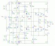
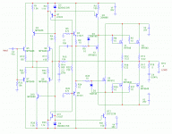
I concentrated on car amps last times and here is one of them. It's supposed to be 'better quality' amp with no bias adjustment, FET output stage and ability to drive 2 Ohm, or 4 Ohm in bridge.
I reminded old style BJT 'parallel' output stage known from Soviet articles of 1980s, and implemented it on FET basis. The input stage is some modified of that kind of old style Japanese amplifiers.
Power supply is SMPS PWM converter with primitive stabilization of rails. Those '10V batteries' on simulation schematic are bootstraps for maximum efficiency.
Measured parameters:
output power: 60W @ 4 Ohm,
or 100W @ 2 Ohm (200W @ 4 Ohm bridged);
THD+N: 0,002% @ 20Hz at rated power;
0,002% @ 1kHz at rated power;
0,036% @ 20kHz at rated power;
0,0015% @ 1kHz at 1W into 4 Ohm load.
Any suggestions about further improvement appreciated!
Attachments
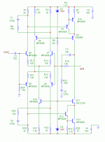
Yep. And in my real p.c.b. there used: Q5=2SD600, Q11=2SB631, X3=IRF9610, X4=IRF610, X1=X2=IRF640, X5=X6=IRF9640.
Two output pairs in parallel because I use single heatsink and silicon insulation.
Bias current is about 200mA each pair and slightly increases during heating.
As soon as I get a photocamera - probably tomorrow - I'll put a p.c.b. photo here.
Two output pairs in parallel because I use single heatsink and silicon insulation.
Bias current is about 200mA each pair and slightly increases during heating.
As soon as I get a photocamera - probably tomorrow - I'll put a p.c.b. photo here.
Banned
Joined 2002
Banned
Joined 2002
I see folks primarily are interested in VAS not in output stage
darkfenriz, I don't know how to call such voltage amplifying stage, so let's call it cascoded.
I think this output stage is claccical AB mode, as total bias current is 400-500mA, as I mentioned above.
It doesn't need bias adjustments as long as specified FETs are used from the same manufacturer (in my p.c.b., I installed random lot FETs by IR). Well I agree that bias in this schematic is dependent on threshold of FETs and hence on different types and manufacturers and can be difficult to decrease if needed.
Here I put the original prototype schematic (some values there may be incorrect though). Common emitter VAS has been replaced for common collector one (it's maybe not obvious from the first sight that it's double emitter follower there). Cascode stages left the same.
The main idea was to lower open-loop gain while trying to expand gain-bandwidth. Simulation shows open-loop gain about 5000 decreasing to 3500 at 20kHz (C3=0). With differential stages emitter resistors increased to 330 Ohm, 2600 and 1800, respectively.
By the way you gave me another idea to connect collectors of Q3, Q12 (my sch references) directly to ground - whether it will be any difference there ot not. By now simulation shows open-loop gain degraded by about 10% because of this.
Attachments
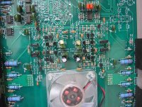
here is its p.c.b. picture. It was first made for higher power amplifier 'conception' with high bias that's why there are some free TO-220 rooms, preamplifier space and even two fans added.
Q1 and Q15 also installed on the heatsink along with all FETs.
I'm aware this p.c.b. is so large that is useless for actual amplifier
Q1 and Q15 also installed on the heatsink along with all FETs.
I'm aware this p.c.b. is so large that is useless for actual amplifier
Attachments
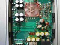
here is its power supply section. By now, I removed DC chokes and rewinded transformer for no-PWM operation; now maximum output power strongly depends on input battery voltage.
Unfortunately, all references on p.c.b. do not correspond to schematics shown (schematics taken from simulation program).
***
why I'm asking for advice? Because amplifier shows THD increase linearly with frequency above 1kHz, although slew rate is about 20V/us with frequency correction shown. And I cannot recognize where is main problem - how to overcome this or how to make gates 'moving faster'. I say so about gates because decreasing of R7, R28 values gave me linear decrease in THD at high frequency! these resistors actually define VAS bias current, but its further rise makes Q5, Q11 very hot (dissipation 1W and more). So I suspect FET gate capacitances to cause this problem.
Attachments
I don't know why it is so.
Maybe you could skip R10 & R25 and increase current though drivers by lowering values of R5 & R34. This could inrease the bias of the output stage, so maybe 0.33 source resistors would be better.
Your problem seems not speed as slew rate isn't low.
I'd rather think small gate resistors of power mosfets can result in slight cross-conduction and unequal turn-on and off times.
You could try 100 ohm gate resistors with no major harm to speed I think.
Wait for specialists' replies.
cheers
Hmm, one version shows a Sziklai pair in the VAS, the other shows a Darlington. What gives ?
Also with either the Sziklai or the Darlington, all that I can get to happen (in simulation) is a nasty sawtooth oscillation at about 5MHz. I'm trying it out with a (tried and tested) Triple Darlington drive stage. I can post a schematic if neccesary.
Cascode VAS has appealed to me since i read peufeu's article on memory distortion, but i've never had a lot of luck with them.
darkfenriz, I tried to short pre-out FETs gate resistors. The result was somehow odd: damaged IRF9610 at the very first power-on. When put back 10 Ohm, no such problems with already hundreds power-ons and offs. Tried also to increase pre-out bias 3 times - R5, R34 down to 47 Ohm. Output stage bias indeed increased, but THD at high freq. remained same. Source resistors increasing won't help too (on the p.c.b. photo you can see source resistors of my first trial even with 1 Ohm - those near free fet rooms - then 0.47, 0.33, finally established at 0.22 Ohm with best result).
jaycee, what simulation program you use? I use Microcap 7. The result is depending on models a lot
No such effect (any sawtooth oscillation whatever) nor in simulation nor in living being I have. Well, Microcap shows a little bit dirty transient with C3=33pF, wich disappears with 47pF there. In reality, square output is perfect without a minor overshoot with 33pF in correction. I'll try to put a capacitor parallel with dummy load and then report results.
Again about VAS, I use common collector-common base BJT connection in there, instead of darlington common-emitter in original.
So that is my mistake to call it cascoded (cascode is common emitter-common base)

And, yes, please post your schematic variant.
I'm thinking now about trying another VAS type with same output FET follower and compare.
jaycee, what simulation program you use? I use Microcap 7. The result is depending on models a lot
No such effect (any sawtooth oscillation whatever) nor in simulation nor in living being I have. Well, Microcap shows a little bit dirty transient with C3=33pF, wich disappears with 47pF there. In reality, square output is perfect without a minor overshoot with 33pF in correction. I'll try to put a capacitor parallel with dummy load and then report results.
Again about VAS, I use common collector-common base BJT connection in there, instead of darlington common-emitter in original.
So that is my mistake to call it cascoded (cascode is common emitter-common base)
And, yes, please post your schematic variant.
I'm thinking now about trying another VAS type with same output FET follower and compare.
You might try the emitter-follower buffered VAS as suggested by Self. It will work similarly to the compund pairs you have now, but in my experience it works slightly better than any other arrangement of two transistors in a VAS.
Mr Evil, thanks a lot for the link. I'll check if there are any new ideas to me. The emitter-follower-buffered stage is familiar for 10 years to me (actually I used it in one of my first amplifiers) but IMO it's far not the best choice...
Marc, of course you MAY doubt, yet it's pretty WORKING in simulator and on my table as well...
Do I give any premise not to trust information given by me above (schematics, parameters etc.) ?
Parameters measured by "Audio precision System One" which I'm lucky to use at laboratory...
Marc, of course you MAY doubt, yet it's pretty WORKING in simulator and on my table as well...
Do I give any premise not to trust information given by me above (schematics, parameters etc.) ?
Parameters measured by "Audio precision System One" which I'm lucky to use at laboratory...
I use LTSpice. Most of the models came from www.onsemi.com
I did eventually get the sim to run stable, but only by adding much R-C compensation that would most likely have completely ruined the slew rate.
I don't doubt that your real-life version works though, it is certainly very impressively and professionally made I dont have the money though to try building things that may very well explode when I apply power though, so I'm playing it safe with tried and true methods for now.
I did eventually get the sim to run stable, but only by adding much R-C compensation that would most likely have completely ruined the slew rate.
I don't doubt that your real-life version works though, it is certainly very impressively and professionally made
I dont have the money though to try building things that may very well explode when I apply power though, so I'm playing it safe with tried and true methods for now.Just made real tests with square wave and parallel capacitor in 4Ohm load. Amplifier remains stable only with 0,1uF in load and shows potential oscillation with ridiculuos 0,22uF there. That's been too disappointing result. After degeneration resistors in differential stage increased to 330Ohm, stability result is better,but... got it! THD+N arises about same two times. Now reminded old truth about evaluating first the same amplifier without negative feedback applied. Finally, I developed input stage similar to what MikeB described in his recent topic (folded cascode - I like the idea a lot), keeping it symmetrical though. I thought this one may give lower distortion without feedback. Also added there BJT follower buffer to decouple gates from VAS. Measurements show distortion about 30-40% higher than first VAS (R5, R28 on schematic removed). With R5=R28=47k, and R14=0 (only DC feedback applied) amplifier shows gain of about 100 within full audio range with distortion 1,3% at 50W/4Ohm and 0,35% at 10W/4Ohm not depending much on frequency. With AC feedback, reducing gain to 20, distortion is 0,09...0,14% in full range at 50W/4Ohm.
Truly, original VAS shows about 2,2...2,7% THD at 50W/4Ohm without AC feedback, not reducing much at 10W. So looks like "folded cascode" originally shows better linearity (while some worse with NFB applied).
Stability of folded cascode is also better - it normally withstands 0,47uF in load (with 33pF in correction).
Also measured alone output FET follower linearity. It shows about 0,2% THD in audio range at 40W/4Ohm (maximum signal that generator allowed), and decreasing at lower signals. Looks not bad.
I will continue researching and trying another input stage. Thanks to all for advices so far.
Attachments
Upupa Epops, thanks. Generally I knew that, just didn't try yet with this amplifier.
Connecting capacitor to the output and feeding amplifier with square signal is some standard test for stability, I heard good designs withstand 2uF in load without ringing at rise and fall transients.
Connecting capacitor to the output and feeding amplifier with square signal is some standard test for stability, I heard good designs withstand 2uF in load without ringing at rise and fall transients.
- Status
- This old topic is closed. If you want to reopen this topic, contact a moderator using the "Report Post" button.
- Home
- Amplifiers
- Solid State
- My 'parallel' amplifier