Hi Andriy,
This temperature rise I would not allow in one of my designs. I have measured this in commercial products sold to average people for music reproduction, and the cases did have a fair amount of ventilation. Clearly not enough.
I was just pointing out that this temperature rise is known to exist inside some brands of equipment. With that high dissipation I would probably change to a TO-220 case and larger heat sink, and / or lower the standing current to drop the dissipation. I've also had the benefit of seeing equipment after many years of operation at higher dissipation levels and the long term damage that can result. Try not to allow high running temperatures. 1 watt can be a lot for a smaller component. Perhaps consider a higher ambient temperature inside the case and assume a problem situation where the temperature runs above 35 °C. That temperature isn't unusual BTW. Assuming these things will reduce the failure rate as that doubles for every 10 °C rise in temperature.
Best, Chris
The ones that run the hottest, unless you happen to be a polystyrene capacitor that is.
All parts have a MTTF rating. Heat accelerates this, so that the ones you would notice first are the ones with the lowest MTTF and are also the hottest. Really, the answer is "it depends". Germanium parts don't like heat for example. Other than this, I can't give you a better answer.
-Chris
All parts have a MTTF rating. Heat accelerates this, so that the ones you would notice first are the ones with the lowest MTTF and are also the hottest. Really, the answer is "it depends". Germanium parts don't like heat for example. Other than this, I can't give you a better answer.
-Chris
At what point does the PCB start to have problems like scorching or smelling bad?
What are the heat related failures that can't be traced to simply exceeding the MTBF/time relationship? For instance traces lifting off the PCB, cracking solder around transistor pins (while the transistor is undamaged), etc.
How can we possibly know what will happen after 20 years of operation?
It's funny that every time someone mentions failures due to high ambient temperature, they conspicuously avoid saying what a good design target would be to avoid such failures.
I guess my main question is this. If you designed an amp where all the transistors had adequate margins to last 20 years at a high ambient temperature, what failures would you see that weren't transistor-related?
Unless a transistor is mistreated, it should not fail early. If a transistor has a MTBF of 5000 hours at 150C, it will last 20 years at 98C. Unless the manufacturers are grossly misleading us of course. Note that MTBF means Mean Time Before Failure, so it is an average. Some fail sooner, some fail later.
I guess I would like to see more meat on this topic, rather than "I put my finger on it and it feels like it will last 20 years".
My point was NOT to fry the amp, i tryed to explain a step input with no feedback to you.Sorry, but I don't understand the point, why would we ever need to short the amp (to ground the output)? Does it really matter what happens then or how the amp will fry?
You dont get it, i wish you good luck.
Yes its flawed or good enough
I would do somthing already suggested, caused by the already several times explained unlinearity that occurs at +/- 0.35 Volt input step and above.
For you its obvius good inough as you argue several times and not looking further into how and why..
Good luck with your further development.
I would do somthing already suggested, caused by the already several times explained unlinearity that occurs at +/- 0.35 Volt input step and above.
For you its obvius good inough as you argue several times and not looking further into how and why..
Good luck with your further development.
Hi keantoken,
The information you are looking for can be had in two ways. One, look to PC board manufacturers to see their data. I don't know if they have data on the abuse of their product. Second, look at older electronics for this damage and that will give you an idea as to what temperatures over time will "cook" a board. I've seen too much of this damage over the years to ignore those lessons.
Equipment you should look at. Most Pioneer receivers, the SX-5 may be the worst for that, and most have the regulator PCB mounted upside down under the chassis. Counterpoint SA-100 amplifiers near the amplifier fuses. Several "high end" tube amplifiers. Generally you can recognise the brown to black patches. Sometimes the substrate de-laminates (epoxy) or even burns through slowly (phenolic). The early Mission product and some class A amplifiers also burn to death. Just use a thermometer to see what the running temperatures are. This is affected by run time also, as well as the quality of the board.
Studer had some problems with the motor servos related to heat and current. They had to add transistors to combat the problem. It was an expensive lesson. Transformers can and do go open due to the thermal fuse opening too. I think that high temperatures over a period of time may make that thermal fuse more sensitive so that the open temperature drops until it reaches the actual run temperature and opens.
You have clear examples of this to look at if you want to, not unless you don't work in failure analysis or as a technician. But the examples of design failures surround us. Another good example would be old Bryson 4B amplifiers. They ran too hot as well. However, I have never needed this data to design or repair equipment. A nomograph would be the best form for this data. All you need is temperature and run time in hours to relate to a failure rate increase. But then do you define failure as complete failure, or trace adhesion failure? Anything in between? Know that the information will be presented in the most favorable light for that material.
Okay, I did a quick search on the internet (Google) for "PC board failure vs temperature" and have a ton of hits. It would seem that the information you seek is readily available.
Best, Chris
I haven't got any projects or builds that have suffered heat damage and my stuff goes back to the mid-70's. Most of that stuff still works today unless they suffered shipping damage or I gave them away.At what point does the PCB start to have problems like scorching or smelling bad?
The information you are looking for can be had in two ways. One, look to PC board manufacturers to see their data. I don't know if they have data on the abuse of their product. Second, look at older electronics for this damage and that will give you an idea as to what temperatures over time will "cook" a board. I've seen too much of this damage over the years to ignore those lessons.
Equipment you should look at. Most Pioneer receivers, the SX-5 may be the worst for that, and most have the regulator PCB mounted upside down under the chassis. Counterpoint SA-100 amplifiers near the amplifier fuses. Several "high end" tube amplifiers. Generally you can recognise the brown to black patches. Sometimes the substrate de-laminates (epoxy) or even burns through slowly (phenolic). The early Mission product and some class A amplifiers also burn to death. Just use a thermometer to see what the running temperatures are. This is affected by run time also, as well as the quality of the board.
Well, that's not realistic. Any transistor that has run that hot long enough to burn the PCB will generally have a shift in parameters. It may not have failed outright yet, but undesirable changes are taking place. A transistor, diode or resistor sitting in a burned area is not going to be healthy. Capacitors are extremely vulnerable to heat related damage.What are the heat related failures that can't be traced to simply exceeding the MTBF/time relationship? For instance traces lifting off the PCB, cracking solder around transistor pins (while the transistor is undamaged), etc.
Experience for one. Older designers have this advantage over new ones. I have not needed to even look for MTBF stats for PC boards as experience looking at the problems is a very good teacher if you care to pay attention to this.How can we possibly know what will happen after 20 years of operation?
It depends on run time in hours for one. This is variable as equipment may have different duty cycles. Some industrial power supplies might be another good place to look. Companies like Hewlett Packard and Lambda seem to be very good at avoiding this type of damage. It's almost like they can see into the future! So you can see it is possible to see even 30 years into the future.It's funny that every time someone mentions failures due to high ambient temperature, they conspicuously avoid saying what a good design target would be to avoid such failures.
Well, again that isn't reasonable since the transistors are badly affected by heat. What you will see is a higher than normal failure rate with the product. Under warranty we were told that heat damage in a product not prone to this was not a warranty situation as it was abuse. I completely agree with them. But other failures will include bad capacitors, resistors that may drift out of tolerance or suffer cap to body failures. Transistors and diodes can go both leaky and / or noisy. There may also be lead to die attach problems that can cause a part to simply go open, possibly intermittently.I guess my main question is this. If you designed an amp where all the transistors had adequate margins to last 20 years at a high ambient temperature, what failures would you see that weren't transistor-related?
Well, the point I made earlier is that the failure might actually be that the part changes it's characteristics. The part has not failed outright, which is how they define failure. It has become unsuitable for the application and generates a service visit or replacement.Unless a transistor is mistreated, it should not fail early. If a transistor has a MTBF of 5000 hours at 150C, it will last 20 years at 98C. Unless the manufacturers are grossly misleading us of course. Note that MTBF means Mean Time Before Failure, so it is an average. Some fail sooner, some fail later.
Studer had some problems with the motor servos related to heat and current. They had to add transistors to combat the problem. It was an expensive lesson. Transformers can and do go open due to the thermal fuse opening too. I think that high temperatures over a period of time may make that thermal fuse more sensitive so that the open temperature drops until it reaches the actual run temperature and opens.
You have clear examples of this to look at if you want to, not unless you don't work in failure analysis or as a technician. But the examples of design failures surround us. Another good example would be old Bryson 4B amplifiers. They ran too hot as well. However, I have never needed this data to design or repair equipment. A nomograph would be the best form for this data. All you need is temperature and run time in hours to relate to a failure rate increase. But then do you define failure as complete failure, or trace adhesion failure? Anything in between? Know that the information will be presented in the most favorable light for that material.
Okay, I did a quick search on the internet (Google) for "PC board failure vs temperature" and have a ton of hits. It would seem that the information you seek is readily available.
Best, Chris
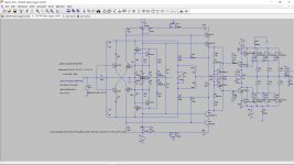
Another solution for predrivers' high Pd is to bolt them to main heatsink.
Could anybody please confirm what R Dijk stated about current input stage?
I've checked my front-end psu with 990R resistors load. Voltage drop across these resistors approximately 38V, which means 38.4mA. The sim shows 53mA current consumption for 4mA bias of input stage and 38.2mA current consumption for 3.1mA bias.
Perhaps this is the reason of my front-end psu voltage sag. Is it possible to increase the power output of my psu?
Last edited:
Another solution for predrivers' high Pd is to bolt them to main heatsink.
Could anybody please confirm what R Dijk stated about current input stage?
I've checked my front-end psu with 990R resistors load. Voltage drop across these resistors approximately 38V, which means 38.4mA. The sim shows 53mA current consumption for 4mA bias of input stage and 38.2mA current consumption for 3.1mA bias.
Perhaps this is the reason of my front-end psu voltage sag. Is it possible to increase the power output of my psu?
Just wondering about your safety system of a light bulb in series with the mains primary. You have two separate transformers - are the primaries for these in parallel or do you have separate light bulbs for each?
Could anybody please confirm what R Dijk stated about current input stage?
I've checked my front-end psu with 990R resistors load. Voltage drop across these resistors approximately 38V, which means 38.4mA. The sim shows 53mA current consumption for 4mA bias of input stage and 38.2mA current consumption for 3.1mA bias.
Perhaps this is the reason of my front-end psu voltage sag. Is it possible to increase the power output of my psu?
This is Ohms law, so EVERYBODY can confirm it.
Do you know Ohms law?
-Resistance multiplied with current equals voltage.
-sum of series voltage equals circuit terminal voltage
-sum of currents equal psu current.
Yes it is possible to increase the POWER OUTPUT from front end power, that has nothing to do with lack of anderstanding or has it?
Just connect a 10 Ohm resistor from positive to negative, that increases the power consumtion and therfore powersupply output. Or what the heck are you on to guess about this time????
Sag ??? in your "practical" pin to pin setup or in simmulation ?
Do you ever simulate your circuit?
Is it your "practical" test or simmulation that you don't anderstand this time?
Do you need so much current passinng the light emitting diode?
why dont you use simple transistor buffered zeener supply to the current sorces when you are already using it as kascode for input ?
No no hold on you may need tenfold of arguing pages before....
Btw: Why have you chosen such unlinear transistors in the region zero-10 ma for input stage ?
Yes, the primaries in parallel, single light bulb. I also tried to connect front-end supply directly to mains with the same result.are the primaries for these in parallel or do you have separate light bulbs for each?
Just connect a 10 Ohm resistor from positive to negative, that increases the power consumtion and therfore powersupply output. Or what the heck are you on to guess about this time????
Was it insulting for you I asked for confirmation of your statement, as I can see from your aggressive post?
This is not my schematic. I'm not familiar with design, that's why I need to ask people who took part in making it to work in simulation.
This is not my schematic. I'm not familiar with design, that's why I need to ask people who took part in making it to work in simulation.
Thought this was yours: look at the name in pictures "SSAHP kplus siggen sim5C"
Change simmulation to transient setting and freq start time and stop time.
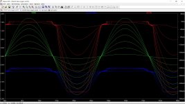
Previus posted simmulation results as picture of this circuit.
Attachments
This circuit if from another abandoned thread.
Do you have an idea why front-end PSU sags? I've checked the voltage after rectifiers before transistors it's 49.8V with load and without load, after transistors 49.5V without load and 39V with load. As this is a shunt psu, input rectified voltage should be higher than the output voltage? Perhaps I need to have 10V higher secondary of the transformer for stable 50V output.
As you previously wrote, anomalies in the current input stage, at current sources cannot be eliminated by design change, only complete redesign of input stage is a solution? Your balanced buffered input is no longer CFA than?
A while back you mentioned some 1k resistors without identifying the part numbers. These appear to be R10 and R11 - putting together a picture from some other measurements the zener diodes associated with this (one being substituted by TL431) these drop voltages of 5V and 15V.
The supply rail feeding the combinations is +/- 39V. From this the voltage dropped by R10 and R11 is 24 V and by applying Ohms law I=V (Volts) divided by R (Ohms) is equal to 24/1000 = 24 ma.
The emitter voltages of Q16 and Q17 will be higher than their respective base voltages so these will conduct depending on the currents drawn through the bases.
At switch on you have observed the initial voltages of the input stage sag over a short time.
If you have a safety bulb in series with your transformer primary the efficiency of this component is reduced and charging of the main capacitor banks and the 1000uF caps in parallel with the 15 V zeners will be somewhat delayed until fully charged.
In this period the voltages at the bases of Q16 and Q17 will be close to those on the relevant supply rails and move apart during the charging period.
You can check this out by measuring the voltage drops at both ends of resistors one at a time with reference to ground - R10,R11,R14, and R15.
If Q16 and Q17 are driven too hard the impacts will be felt in the stages that follow. This is likely to be contained by the strictures of the light bulb on available current for the front end as well as the power stages. Nonetheless leave that in place for now.
The way to regulate base conduction in Q16 and Q17 depends on the values of R10 and R11. 2.2k would be a better choice - see what impact that has.
Not exactly. If you mean I mentioned some 1k resistors from post 709, this is stand alone testing of frontend psu without amp with help of 1k resistors. However R10, R11 on the pcb are the same. Zeners on the amp drop voltages, for example, from initial 49V input at 5V zeners to 44 Volts, which appears to be at bases of Q16, Q17, and to 15 Volts at 15V zeners. All these can be checked in the sim.
Light bulb has nothing to do with the sag (which is also present with frontend psu connected directly to mains) which is constant not only in charge time.
R10, R11 values are just right. If you check the sim I can raise them to 1.1k only to maintain 15V at D1, D2. With 2.2K there won't be 15V potential, only just 7-10V.
As I mentioned in previous post, more likely psu sag appears from not proper input voltage setting to shunt psu which my frontend is. Output voltage of shunt psu cannot be the same as it's input voltage.
Shunt psu, now you may have an high output resistance....
In witch post is your correct circuit with correct values ?
This Lazy cat circ do have the same issues whatever input trannies you are using. Yes i understand its not yours its your friends circ. The same you tried to fault trace for ore than a year without results?
Sorry to see somone using this topology. the input circuit is a bad topology.
- Status
- This old topic is closed. If you want to reopen this topic, contact a moderator using the "Report Post" button.
- Home
- Amplifiers
- Solid State
- One of the Top Solid-State CFA amp design