AN approach that seems to work is to limit the input stages to two gain stages only - e.g. input differential and differential, Darlington VAS stage, with triplet output stages. Global NFB with phase lead from the output works with RC phase lag on the outputs of the differential input stage, and VAS output stage. However there may still be some slight, damped, internal ringing, which can be completely cured by taking the compensation from the VAS stage to the feedback point instead of the output connection. The 20kHz may increase to about 0.01% but THD is around 0.002% at 1kHz, lower if the global approach is used.
What is your simulation show, will it work or Mjona is right in his experience?
What is your simulation show, will it work or Mjona is right in his experience?
What John has described is a fresh design approach so when you ask "will it work" does this mean an entirely new circuit or applying John's ideas to the present one?
I looked at compensation on the basis of not departing significantly from the Lazy Cat design and showed that adopting John's proposed method would not work in this particular instance due to the snag of an additional pole to the two that already existed in the Vas and the first transistor in driver stage also having some voltage gain.
The other option without going to a complete redesign would be to rearrange the output into the form of a three stage emitter follower -which eliminates the added frequency pole mentioned in my last post.
With these changes the circuit delivers a THD which is on a par with my most recent simulation.
I was under the impression you want to stick as closely as possible to the original Lazy Cat structure.
I have not posted the simulation as it is not clear now what your design aims are and this is beginning to look like a competition where the entrants do all the work and there is no final result.
What John has described is a fresh design approach so when you ask "will it work" does this mean an entirely new circuit or applying John's ideas to the present one?
I was under the impression you want to stick as closely as possible to the original Lazy Cat structure.
I have not posted the simulation as it is not clear now what your design aims are and this is beginning to look like a competition where the entrants do all the work and there is no final result.
Preferably accomodating John's approach with present circuit, however entirely new circuit won't be a harm to my aim) while it provides high frequency responce, low output impedance, high slew rate, simple schematic (for small pcb) and low distortion, which can be achived with CFA design.
I don't insist to stick as closely as possible to the original LC structure, I just don't want HF responce to be killed with inductive add-ons.
Also my aim is to use components I currently posses, however using mosfets in drivers stage might be beneficial.
Thanks for clarifying the flexibility with your design aims, I will post my EF 3 simulation later.
In regard to your comment about HF response being killed with inductive add-ons, any effect with audio would show up in the THD results for a 20 kHz sine wave test signal.
If the error result is neglible you can forget the idea of any impairment being due to inductive add-ons.
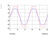
We don't listen to square wave test signals a 10 kHz one is used to see how well the feedback loop works - this will be at extreme high frequencies before a point where phase changes arise ahead of a drop in output level.
Thanks for clarifying the flexibility with your design aims, I will post my EF 3 simulation later.
In regard to your comment about HF response being killed with inductive add-ons, any effect with audio would show up in the THD results for a 20 kHz sine wave test signal.
Thanks for your kind support. I understand in some designs it's impossible to omit output coil as a safe margin with different load. What I wrote about add-ons is a preference only.
Here is a simulation (sorry for the poor quality) of my 100W design using global feedback compensation at just over 100W and clipping as simulated. 100W distortion at 20kHz is 0.0016%. Still to be build and verified, however, the previous version achieved 0.003% at 20kHz, measured. (FET means FET input stage.)
Attachments
Yes, I am referring to using FETs in the input stage. But I'm not saying they are better, necessarily. I use FETS so that I can have D.C. frequency response (no electrolytics in the feedback path nor any capacitors to cause distortion in the audio band). I have used BJT's too but they are better with A.C. coupling and feedback because of the bias currents needed. I have designed a bias compensating circuit for D.C. application but not tested it and suspect it may introduce a noise current, but that might only appear when the amplifier is disconnected from a preamp.
I'll have to take another look at the LC design to comment.
I'll have to take another look at the LC design to comment.
Hi AndriyOL, I took a fast read at the thread.
As I told in the emails, there is no way to make a "current feedback" input stage with balanced high impedance inputs.
In a "current feedback" input stage there are 2 input nets. One of the input nets is low impedance, the other is high impedance.
Implementing high impedance balanced inputs with a "current feedback" input stage requires a buffer stage:
a) Summing its output in form of current to the low impedance net. Non-inverting buffer.
b) Summing its output in form of voltage to the high impedance net. Inverting buffer.
(End of list.)
The whole point of current feedback inputs seems largely misunderstood in audio. Where is the extra "speed" coming from? It comes from eliminating one gain element from the feedback path, so propagation delay and phase shift are reduced, allowing for highest GBW for a choice of part types.
In high speed current-feedback op-amp design (where state of the art of linear amplification is currently expressed, not so much in audio), typically IN- input current goes straight (through input transistors acting as cascodes) to drive VAS. LTP phase shift and delay are eliminated from IN-. This can represent an improvement of 33%, as in 3 gain stages becoming 2 (counting output stage as 1 gain stage). These op-amps are available with GBW of over 100Mhz, made with transistors exhibiting unity gain FT as high as 8Ghz. These op-amps are often used for video signals.
For audio linear amplification, while it is certainly advantageous to increase GBW, the delay and phase shift associated with VAS and output stage can be an order of magnitude higher than what is gained by removing the delay and phase shift from half LTP. On the other hand, balanced inputs for simple amplifiers, or bridging, are trivial to make with LTP input stages.
What has to be understood about linear amplification is that:
- There is a logic to derive the circuits. There is a logic that describes the few optimum possible circuits. This is Abstract Algebra.
- There is a physical limit to the performance that can be obtained for every set of part types, and amount of each part, chosen.
- When increasing the amount of part types, or the amount of each part, the slope of the function "measured_results(n_types,n_parts)" starts positive but becomes zero, then negative. Past a certain point, more parts are loss, best part types are already into use, the right amount too.
- Previous principle is also true for semiconductor design and production. Materials have a theoretical limit. The limit was reached.
I have never used FET's in amplifier input stages - to match pairs from single devices -say for an LTP - one might need a dozen or more samples.
Dual FET's on the same chip are a solution but you might need to put in a special order and be prepared to pay at a premium.
I am not against FET's per se.
Recently I saw a Conrad Johnson Sonographe CD player for sale in a shop and bought it on the spot.
This is a dressed up version of a 14 bit Phillips/Magnavox CD350 player which was the first player I ever bought.
It the CJ has wooden cheeks and a fancy front panel but inside there is a special board with a single FET replacing the final filter stage.
What a difference this makes.
JFET in audio are one of the elements that are not introduced almost until everything else has been tried.
JFET have moderate gain in the form of voltage to current conversion. In comparison to a bipolar transistor, a JFET needs a few volts of swing of input signal to achieve the full swing of drain current. Bipolar transistors can do the full swing of collector current with just 500mV p-p input. (This is considering that current has to fall to microamperes.)
JFET have very low input capacitance, and negligible input current.
JFET are used in 3 fields:
- High frequency amplification, as in oscilloscope input stages and RF tuners.
- High impedance amplification, as in multimeters and JFET op-amps.
- Modulation: a saturated JFET works as a variable resistor, limited to about a half diode drop +/-250mV before distortion makes it less and less useable.
Audio amplifiers with JFET at the inputs have stability phase shift (a.k.a. phase margin, <45deg) achievable up to a higher GBW, due to the fact that input impedance to a bipolar LTP decreases with frequency, becoming the 1st contributor to HF roll-off, while the JFET LTP does not exhibit that roll-off until >10x higher frequency.
Additionally, the JFET LTP copes well with a 2nd bipolar LTP gain stage, degenerated to maximize GBW and provide only the remaining gain, to match the gain of a normal bipolar LTP.
Additionally, JFET LTP copes better with HF/RF hash at the inputs.
Concerning the CD player, I suppose they found that a JFET preamp was well matched to the old 14-bit DAC chip.
Hi AndriyOL, I took a fast read at the thread.
As I told in the emails, there is no way to make a "current feedback" input stage with balanced high impedance inputs.
Implementing high impedance balanced inputs with a "current feedback" input stage requires a buffer stage:
a) Summing its output in form of current to the low impedance net. Non-inverting buffer.
b) Summing its output in form of voltage to the high impedance net. Inverting buffer.
(End of list.)
On the other hand, balanced inputs for simple amplifiers, or bridging, are trivial to make with LTP input stages.
Hi Eva. Pleasure to read your contribution in this thread. I remember you are interested in a technical discussion.
Could you please show how to implement a buffer stages to this schematic? Perhaps it will be simpler and more beneficial with JFETS input stage. I have a bunch of BF862. Can they be used for input stage? However they are only n-channel and there seem to be no p-channel complementary like with 2sk170 part
Last edited:
Another advantage of JFETs is that because of the increased voltage swing needed they are unlikely to suffer from being cut-off in high frequency signals. I think that was covered in Eva's comment about HF/RF hash but not explicit.
You can achieve a similar performance with BJT's using emitter degeneration, otherwise I've usually taken +-120mV as the maximum swing for an LTP, this being twice the 60mV which changes the current in a bipolar by 10x. And a 10x change in current is well past linearity; except of course there is cancellation of even harmonics in the LTP which keeps them a bit more linear over a wider range.
I use only n-JFETS in the input stage, not a complementary LTP. No need for bias current compensation - the main reason I use FETs. I used BF244's, but would have to consider BF545 version now. The BF862 has a higher gain, and at 40mS would be similar to BJT's at 1mA. That would be interesting to explore, but may need source degeneration to increase the input voltage swing tolerance and reduce the gain - at the end of the day it is GBP that determines stability etc.
Last edited:
Yes, I'd agree. To obtain matching JFET's it is helpful to buy in one Idss group (I usually use B) and the usual buy a few more than needed. Out of the last group of about 20 devices I managed about 6 pairs with Vgs within about 0.1V at the operating current.
Sadly TO-92 JFETS seems to have gone the way of old metal can stuff into the bin marked obsolete/unobtainium. Matching SMD devices is a tricky task...
Sadly TO-92 JFETS seems to have gone the way of old metal can stuff into the bin marked obsolete/unobtainium. Matching SMD devices is a tricky task...
I have never used FET's in amplifier input stages - to match pairs from single devices -say for an LTP - one might need a dozen or more samples.
Dual FET's on the same chip are a solution but you might need to put in a special order and be prepared to pay at a premium.
I already have a matched pairs of BF862. No problems so far, if the JFETS to be used in input stage
2N5196 is apparently discontinued. I have a few of these from a project with military and these have military specs. Almost 100% match. Following design objectives for instrument amps - such as oscilloscopes- almost nothing compares. But in terms of audio amps ... a bit like crushing flies with canonballs. Over-engineering
A 1ppm amp
Hi Eva,
Thanks for pointing this out. But did you mean 100GHz GBW? I read a paper by Barrie Gilbert where he mentions 64GHz GBW for a 2 stage CFA with feedback (using a 25GHz process) here at p95. Copy of p95 attached.
Your point about dropping one 'half' of the LTP in a CFA to "eliminate" phase shift from IN- is a very significant step for audio power amplifiers.
There was a thread using a "Singelton" input stage by Bigun (with an ingenious temperature compensation idea for the single input transistor) and says, "The Singleton can be easier to stabilize, so Cdom can be smaller and slew rate is higher."

There is also Mike Renardson's MJR7 Mk5 that eliminates the input stage and uses a CFP for the VAS and shunt feedback. His VAS (cum input stage) has a gain of 200,000 (not a misprint) up to 3kHz (see footnote here) giving it a GBW of 1.6GHz. Mike says, "... by excluding the usual differential input stage to reduce the total number of stages, the MJR7 can still use high global loop gain without stability problems."
Mikes MJR7 Mk5 was built by diyAudio member Forr and Mikes distortion readings were verified as correct and "are on the par with those of the best circuits published all over the world." Mike's distortion test results are here. Forr's tests (English translation) can be read here. At 1W it gives a genuine 1ppm at 1kHz and 10ppm at 20kHz -- actual bench tests, not a simulation.
So if we eliminate the phase shift from the first stage it is a very significant step for audio power amplifiers. Thank's again Eva for pointing this out.
Unfortunately, with only one or two examples so far we don't have many buildable amplifiers using this approach to recommend for first time builders. Hopefully that will change.
Hi Eva,
...The whole point of current feedback inputs seems largely misunderstood in audio. Where is the extra "speed" coming from? It comes from eliminating one gain element from the feedback path, so propagation delay and phase shift are reduced, allowing for highest GBW for a choice of part types.
In high speed current-feedback op-amp design (where state of the art of linear amplification is currently expressed, not so much in audio), typically IN- input current goes straight (through input transistors acting as cascodes) to drive VAS. LTP phase shift and delay are eliminated from IN-. This can represent an improvement of 33%, as in 3 gain stages becoming 2 (counting output stage as 1 gain stage). These op-amps are available with GBW of over 100Mhz, made with transistors exhibiting unity gain FT as high as 8Ghz. These op-amps are often used for video signals.
Thanks for pointing this out. But did you mean 100GHz GBW? I read a paper by Barrie Gilbert where he mentions 64GHz GBW for a 2 stage CFA with feedback (using a 25GHz process) here at p95. Copy of p95 attached.
Your point about dropping one 'half' of the LTP in a CFA to "eliminate" phase shift from IN- is a very significant step for audio power amplifiers.
There was a thread using a "Singelton" input stage by Bigun (with an ingenious temperature compensation idea for the single input transistor) and says, "The Singleton can be easier to stabilize, so Cdom can be smaller and slew rate is higher."
There is also Mike Renardson's MJR7 Mk5 that eliminates the input stage and uses a CFP for the VAS and shunt feedback. His VAS (cum input stage) has a gain of 200,000 (not a misprint) up to 3kHz (see footnote here) giving it a GBW of 1.6GHz. Mike says, "... by excluding the usual differential input stage to reduce the total number of stages, the MJR7 can still use high global loop gain without stability problems."
Mikes MJR7 Mk5 was built by diyAudio member Forr and Mikes distortion readings were verified as correct and "are on the par with those of the best circuits published all over the world." Mike's distortion test results are here. Forr's tests (English translation) can be read here. At 1W it gives a genuine 1ppm at 1kHz and 10ppm at 20kHz -- actual bench tests, not a simulation.
So if we eliminate the phase shift from the first stage it is a very significant step for audio power amplifiers. Thank's again Eva for pointing this out.
Unfortunately, with only one or two examples so far we don't have many buildable amplifiers using this approach to recommend for first time builders. Hopefully that will change.
Attachments
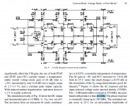
EF2 derivative of the Lazy Cat circuit.
The voltage gain parts of this circuit are weighed down by having three sets of output power devices - the greatest capacitance in a power transistor is that between the base and emitter which with three sets is a liability.
The bandwidth of individual output devices holds up to 3-4 amperes which is adequate for a power output of around 40 watts into 8R. With fuse protection in the supply rails the current handling of a single output pair is adequate.
It is then easier to devise a layout where the half wave currents cancel than with multiple sets.
As far as THD with 30 volts peak sine output at 20 kHz into 8R and any parallel capacitor load of 100n or lower = < 0.0024 % this increases to 0.0153% with 2uF in parallel with 8R.
The equivalent simuation figures for the CFP drive with 3 output sets are <0.0124% and 0.0279%.
I have substituted some Cordell device models in place of a couple of others. The dot include statement on the schematic is linked to Cordell's website which provides some other models to choose if one wishes to test confirm or replace those originally provided.
In the EF2 the currents flowing through Q14 and Q16 have some spikes in the wave forms these are fed back to the inverting input via C34 and the amplifier output is clean.
I thought I should bring this to attention in view of some doubts recently expressed.
I have tried video op.amps in pre-amp stages that which I had was claimed to use Class B inputs - I am happy to take whatever does the job. This device did but my final choice was for an audio grade op.amp.
As a matter of contrast there are no spikes in Q14 and Q16 in the CFP drive circuit which uses Miller compensation.
See also the EF2 zobel capacitor currents where C6 equates to zero current thus zero volts.
In the EF2 I have added V4 which for this simulation represents a dc servo amplifier such as an LF351. I have some concerns about the low values of R4 and R6 being hard to set the dc offset alone and maintain this under dynamic conditions.
The EF3 simulation showed double the distortion of the EF2.
Attachments
- Status
- This old topic is closed. If you want to reopen this topic, contact a moderator using the "Report Post" button.
- Home
- Amplifiers
- Solid State
- One of the Top Solid-State CFA amp design