I have been looking at the bootstrap cap in simulation. This one also seems it would benefit from being significantly bigger! With the standard 220u coupled with a 220ohm to the rail gives really odd currents though the outputs at the start and end of the LF transient (using 4cycles of 20Hz), and the the currents through the outputs also move out of phase at LF because of the capacitor. This causes premature clipping at low frequencies. Going to 1000u is a lot better, but this of course depends on the resistor to rail too.
All these big caps seem to create a long startup before everything is stable, so I guess a delayed speaker relay would be needed, and with a resistor to charge the output cap if there is one.
All these big caps seem to create a long startup before everything is stable, so I guess a delayed speaker relay would be needed, and with a resistor to charge the output cap if there is one.
Last edited:
Some bootstraps if connected to complimentary feedback pair circuits can reach critical positive feedback levels. The 93% of a typical 1960s amplifier seemed OK whilst 97 % not. The cure was a simple series resistor. Whilst the JLH is different it might be doing similar things. 50% positive feedback already does a good job.
Try 10 uF
Try 10 uF
10u on the bootstrap causes severe clipping on the positive side, because the current stays almost constant through the upper transistor, it is hardly modulated at all at LF. I guess that's what they would call single ended class A?
A big bootstrap capacitor and some tuning of the resistors gets the current modulation to mirror the lower transistor, and increases output.
A big bootstrap capacitor and some tuning of the resistors gets the current modulation to mirror the lower transistor, and increases output.
Last edited:
Member
Joined 2009
Paid Member
Would you please enlighten me? I know the startup and maybe shutdown gets problematic, and would probably require a speaker relay. Once up and running it should be ok I guess?
Based on the simulations I've done on LF bursts etc, I would add a zero to the cap values in the original design as thumb rule.
Based on the simulations I've done on LF bursts etc, I would add a zero to the cap values in the original design as thumb rule.
Mike/fredbloggstwo:
I'm looking at your spice model, and getting a bit curious..
If I was to try it with single outputs, do you think it would be ok to leave out the 0,1 Ohm resistors? Or are they there for more than load sharing between the paralleled output transistors?
I'm looking at your spice model, and getting a bit curious..
If I was to try it with single outputs, do you think it would be ok to leave out the 0,1 Ohm resistors? Or are they there for more than load sharing between the paralleled output transistors?
Mike/fredbloggstwo:
I'm looking at your spice model, and getting a bit curious..
If I was to try it with single outputs, do you think it would be ok to leave out the 0,1 Ohm resistors? Or are they there for more than load sharing between the paralleled output transistors?
I would leave them in.
The only time I have seen them left out is for lateral mosfets.
They give a little degeneration and stability.
Mike/fredbloggstwo:
I'm looking at your spice model, and getting a bit curious..
If I was to try it with single outputs, do you think it would be ok to leave out the 0,1 Ohm resistors? Or are they there for more than load sharing between the paralleled output transistors?
A good point: I would be inclined to leave them in circuit myself, however removing them would allow the output devices to get closer to the rails and thus, give a slightly higher output voltage for a single output 'device', but not that much. (2 Amps through 0.1 Ohm is 0.2 Volts)
Try it out and see: thats the beauty of simulation.
") I would expect the distortion to rise a tad without them as they do give a small amount of local feedback.
I would expect the distortion to rise a tad without them as they do give a small amount of local feedback.Note that there is another variation on the same theme which is to use one BD139 to drive two MJ15004s in parallel (with Emitter resistors).
I haven't tried that and was hoping that giving a working Sim would encourage other contributions like your own.
Regards,
Mike
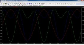
Looking at the currents in the sim something seems odd, if I plot the currents through an upper and lower output transistor, it seems the current sharing is a bit off somehow. Maybe I need to be educated again
Doing this on the standard JLH gave some pretty nice looking opposing current sine waves.
Doing this on the standard JLH gave some pretty nice looking opposing current sine waves.
Last edited:
Another question: should the feedback cap be tied to negative rail? Ok in simulation, but probably not good in a real amp with ripple etc?
Good catch
. The bottom of the 470uF feedback capacitor should be connected to the ground near the input - my mistake.In practise, I think that this would have produced a significant hum.
With regards to the upper and lower currents I am not sure why they may be different. Checking the DC operating point, they all seem to be about 2.36A through the MJ15004s. Maybe its LTSpice being a bit erroneous somewhere. I would think that with the output being at 0 volts DC under no signal, the upper and lower currents should be identical.
If you change R13 to 1K6223, the DC offset goes to 671uV and the upper and lower currents are equal to within a knat's XXX
Mike
Last edited:
I have not looked at currents at idle, but when you feed it a signal and plot the current trough an upper and lower output device, that's when it gets confusing to me.
Output is fine, and it also seems the PS current is fine, so it's not creating extra heat, only the waveform looks odd. Maybe an academic problem, since it seems to work fine, but I would like to understand why..?
I attached the plot and schematic here for reference. The plot has output voltage and currents through one upper device and one lower.
Attachments
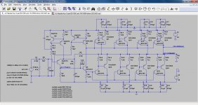
The division of current between the two output halves in the original JLH depended on the two devices having similar gains. The increase in the base current of one device was achieved by pulling current from the other. In this arrangement it seems to me that there is an imbalance between the lower and upper driving impedances. The lower devices have a 2.2k resistor while the upper have nothing but high impedances. That is one of the issues I came across in designing a push-pull with driver transistors.
My immediate reaction is to add the emitter resistors to the BD139C emitter/PNP collector terminals instead of in the PNP emitter, and add a 2.2k resistor between the upper base connections and the centre rail. The VAS stage may need some current adjustment to allow for this.
It may increase the distortion, but with a Sizklai pair Vbe differences won't amount to much as a Darlington would.
BTW I've not seen a BD139C. Are you sure you mean this? The "C" usually refers to 100V spec, such as BD239C.
But the BD139 should handle 100V according to the original spec (BVcbo) but this is not what ST's datasheet says now.
Last edited:
Here is something with inspiration from John. Something like a hybrid of old and new, and it seems to share the currents nicely between the upper and lower outputs now.
Mike, can you please have a look at the details of distortion etc? I have not done more tests than just looking at the currents.
When it comes to component selection, I think Mike should be able to answer, since it's his baby
Edit: I see now I changed the Iq while I was testing different setups, and forgot to change it back. R1 at 500Ohm seems to be ok for the selected load.
Attachments
Last edited:
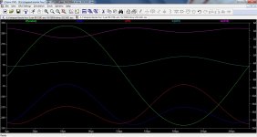
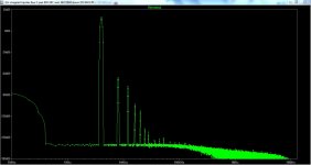
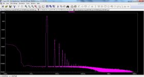
I did a simulation run with both versions with 1V 4kHz (Mike used 4k so I did too) input and then ran a FFT on the output. Both look very similar, and distortion looks decent too (abt 80dB to the 2nd and falling from that), but I guess simulation and real life can differ quite a bit. I think have people suggested reality is better than simulation when it comes to the JLH amp?
Pink plot is the original, and green the strapped version.
Pink plot is the original, and green the strapped version.
Attachments
Last edited:
I am building the JLH Geoff Moss high current Version JLH:
The Class-A Amplifier Site - A JLH Amp for the Quad ESL57
I took the PCB from PaulB and had it produced.
https://www.diyaudio.com/forums/att...lh-10-watt-class-amplifier-geoff-moss-jlh-zip
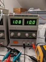
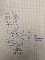
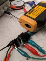
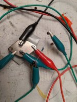
Now I am about to match Transistors (i bought: Q1, Q1a, Q2, Q2a: MJ15003, Q3:1xBD139-16, Q4, Q5, Q6, Q7 BD560c, Q8:BD 140). I've read a lot about that and it never got really clear how to do it. So I just connected as it seemed to make sense for me to my Lab-PSU and measured voltage, current and temperature. I had to stick tape on the Transistor, otherwise the IR Sensor doesn't capture the temperature on the shiny metal. I used a voltage of 10V connected the base of the transistor via 1000 Ohm resistor, which means a current of 0,01 A to it. I wait until the transistor heats up to 85°C and then i compare to the amout sent by the PSU and calculate the amplification. Example: PSU 1,08A = current gain = 108. See Photos.
My Questions:
Does it make sense to measure that way?
Which is a acceptable difference between transistors, to be considered as "matched"
Are there other Factors to be considered/ measured?
I dont get the differece between b560 and b560c in the schematic. Is it ok to use b560c for all Q4-Q7 or do i have to make a difference?, or select appropriately by current gain?
What do you think/ know? Thank you very much for your help!
The Class-A Amplifier Site - A JLH Amp for the Quad ESL57
I took the PCB from PaulB and had it produced.
https://www.diyaudio.com/forums/att...lh-10-watt-class-amplifier-geoff-moss-jlh-zip
Now I am about to match Transistors (i bought: Q1, Q1a, Q2, Q2a: MJ15003, Q3:1xBD139-16, Q4, Q5, Q6, Q7 BD560c, Q8:BD 140). I've read a lot about that and it never got really clear how to do it. So I just connected as it seemed to make sense for me to my Lab-PSU and measured voltage, current and temperature. I had to stick tape on the Transistor, otherwise the IR Sensor doesn't capture the temperature on the shiny metal. I used a voltage of 10V connected the base of the transistor via 1000 Ohm resistor, which means a current of 0,01 A to it. I wait until the transistor heats up to 85°C and then i compare to the amout sent by the PSU and calculate the amplification. Example: PSU 1,08A = current gain = 108. See Photos.
My Questions:
Does it make sense to measure that way?
Which is a acceptable difference between transistors, to be considered as "matched"
Are there other Factors to be considered/ measured?
I dont get the differece between b560 and b560c in the schematic. Is it ok to use b560c for all Q4-Q7 or do i have to make a difference?, or select appropriately by current gain?
What do you think/ know? Thank you very much for your help!
Attachments
- Home
- Amplifiers
- Solid State
- JLH 10 Watt class A amplifier